0
\$\begingroup\$

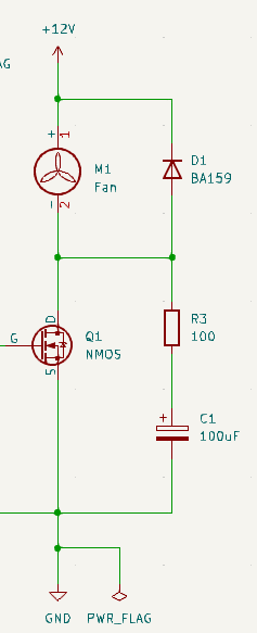
enter image description here

In order to minimize ringing when switching the mosfet, I had to implement an RC snubber circuit. Now, in that case, is the flyback diode still required?

Also, I measured with an oscilloscope the signal across the fan, and also across the mosfet and noticed no difference in both cases (RC snubber with and without diode).

\$\endgroup\$
3
  • 1
    \$\begingroup\$ What current does the fan consume when it is ON? \$\endgroup\$
    – sai
    Commented Sep 8 at 14:44
  • \$\begingroup\$ The fan consumes 0.15A \$\endgroup\$ Commented Sep 8 at 15:02
  • \$\begingroup\$ The question should be: Is a snubber needed when there is a flyback diode? 😉 Answer: "usually not" \$\endgroup\$
    – tobalt
    Commented Sep 8 at 16:10

1 Answer 1

1
\$\begingroup\$

is the flyback diode still required?

It might still be required.

From comments you said that the fan took 150 mA and, because a fan has some inductance, when the MOSFET deactivates you will see a peak voltage at the MOSFET drain of 150 mA × 100 Ω = 15 volts. That is 3 volts higher than the positive supply rail (12 volts). If the diode were present than it will clamp the back-emf to around 12.7 volts.

But because we are dealing with such low voltages it doesn't really matter. A 20 volt rated MOSFET would be adequate for both scenarios but, if your snubber resistance were (say) 150 Ω then, the peak voltage seen at the MOSFET drain would be 22.5 volts and exceed the MOSFET voltage rating.

If the fan took an amp whilst running up to speed and, the MOSFET deactivated during that period then, the peak voltage across the 100 Ω snubber resistor would be 100 volts.

So, it's down to the fine details as to whether you need a diode or not. You might need both because the snubber does slow ringing down and may reduce the EMI produced.

\$\endgroup\$
7
  • \$\begingroup\$ Note the diode is most effective when a bypass capacitor is placed nearby (+12V to GND). \$\endgroup\$ Commented Sep 8 at 18:43
  • \$\begingroup\$ I think that's a red herring. The current in the inductance of the wound device finds a local circulatory path via the diode and a bypass capacitor is irrelevant. Please review what you are saying or justify why you think it's important. \$\endgroup\$
    – Andy aka
    Commented Sep 8 at 19:47
  • \$\begingroup\$ Wire doesn't have to be looped around to exhibit inductance, In fact inductance is a necessary consequence of nonzero length. The Q1-D1-cap loop can still generate peak voltage, worth noting as we don't know how long that +12V connection is here, it might be 10mm or 10m. More comments along these lines here: electronics.stackexchange.com/questions/175390/… \$\endgroup\$ Commented Sep 8 at 21:16
  • \$\begingroup\$ That makes no sense. Maybe it's time to explain how the capacitor proposed in your comment helps. \$\endgroup\$
    – Andy aka
    Commented Sep 8 at 23:47
  • \$\begingroup\$ Andy, I'm not sure what more I can explain; I know you know about this, you're no stranger to SMPS design, and you would never suggest to build say a boost converter without the output capacitor placed nearby. Somehow, I am patently unable to communicate this idea to you here, but I cannot ascertain why. (Could someone else perhaps comment what I'm missing?) \$\endgroup\$ Commented Sep 9 at 0:06

Your Answer

By clicking “Post Your Answer”, you agree to our terms of service and acknowledge you have read our privacy policy.

Not the answer you're looking for? Browse other questions tagged or ask your own question.