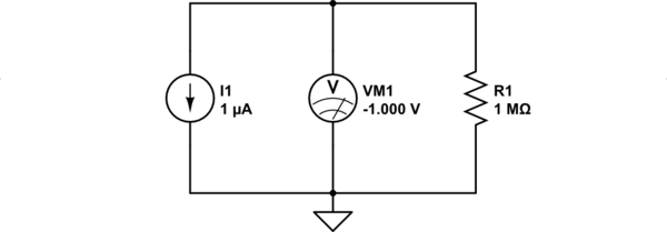
If you "push" 1μA through an energy sink, like a resistor, then you would expect potential to be higher where current enters that sink, and lower where it exits. However, the photodiode is a source of energy, energy derived from incident photons, so \$I_P\$ flowing downwards through the photodiode in your first schematic would cause its cathode to fall in potential, not rise:

simulate this circuit – Schematic created using CircuitLab
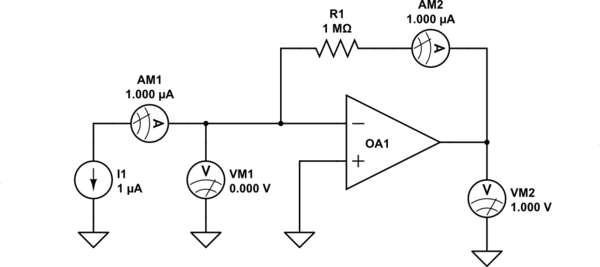
To maintain a virtual 0V at its inverting input, the op-amp would would have to produce a positive output potential:

simulate this circuit
This design is OK for any op-amp that claims to have inputs that work right down to their negative supply potential (0V here), since the op-amp's output can't be anything but positive. The issue you have is with the output, not the input. If the op-amp claims to have a rail-to-rail output, or an output that "includes 0V", it's a lie. You'll always "lose" the bottom few millivolts, or tens of millivolts. That's why you'd want to bias the op-amp to have an output near +0.1V, for instance, so that the output can actually change in response to any deviation in photo-current right down to 0A. You just need to write software to account for the +0.1V offset.
Your second "biased" circuit uses R1 and R2 to provide that offset, but typically you wouldn't want \$\frac{V_{CC}}{2}\$ there, +0.1V is sufficient as I just explained. With \$V_{CC}=+3.3V\$, to obtain +0.1V at the op-amp's input and output, when photo-current is 0A, solve this:
$$ 0.1V = V_{CC}\frac{R_2}{R_1+R_2} $$
That design uses \$V_{CC}\$ to derive bias potential, with the consequence that any noise on that supply is directly injected into the signal, albeit attenuated by a factor \$\frac{R_2}{R_1+R_2}\$. The smaller that fraction, the less noise is injected, so biasing at +0.1V is going to be far less noisy than biasing at \$\frac{V_{CC}}{2}\$. Also, you'd usually mitigate noise with a capacitor in parallel with R2, notably absent in that drawing.
Ideally you don't want any noise, so I would never recommend using \$V_{CC}\$ directly in this way, unless you know \$V_{CC}\$ to be sufficiently stable over time and temperature, and clean, or if the ADC also uses \$V_{CC}\$ as its reference. Better use a zener diode or precision regulator to get a pristine reference potential, and (optionally) divide that down to +0.1V.
A zero-biased photodiode has zero dark current, eliminating the need for offset compensation. While your second circuit solves the op-amp's limited input/output range, it unfortunately introduces a slight reverse bias to the diode, along with the associated dark current, which I'll explain in a moment. Reverse biasing might be a good thing; it increases the width of the diode's depletion region, which decreases its capacitance, and improves performance at high frequency.
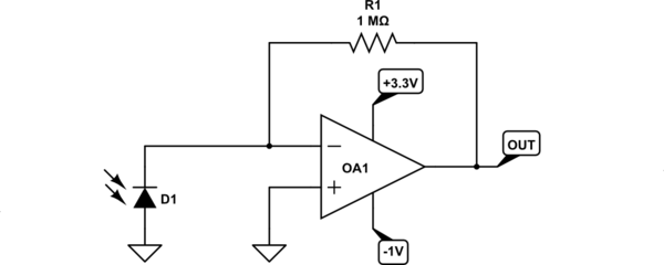
For zero dark current, the most obvious fix to your first circuit is to provide a truly negative supply to the op-amp, while still using the common 0V of ground to zero-bias the diode:

simulate this circuit
It doesn't need to be -3.3V or even -1V, it need only be enough to allow the op-amp to actually output a solid 0V. Even -0.1V would be enough! Check out the LT1054, a switched-capacitor charge pump converter with regulated output, although that will require at least a +3.5V supply.
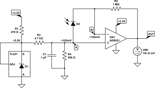
It's still possible to obtain zero-bias on the diode without a negative supply, but you require a low impedance source of +0.1V, or whatever potential you choose. Here's a way to obtain a rock steady +2.5V using the fantastic and cheap precision regulator TL431, and then divide it down to +0.1V:

simulate this circuit
In your second circuit, the junction of R1 and R2 has potential \$V_A\$, and negative feedback ensures that the inverting input has the same potential. Therefore the diode's cathode also has potential \$V_A\$ while its anode is at 0V, so the diode is reverse biased by amount \$V_A\$, causing dark (leakage) current. By contrast, in my circuit here node A is a source of +0.1V, with impedance close to 200Ω, low enough that we can tie the photodiode anode to the same source that biases the op-amp. With negative feedback ensuring \$V_B=V_A\$, the diode has 0V across it at all times, eliminating dark current.
With the help of C1, the TL431 ensures that there's practically no supply noise present at A, and +0.1V at OUT really does mean zero illumination of the diode.

