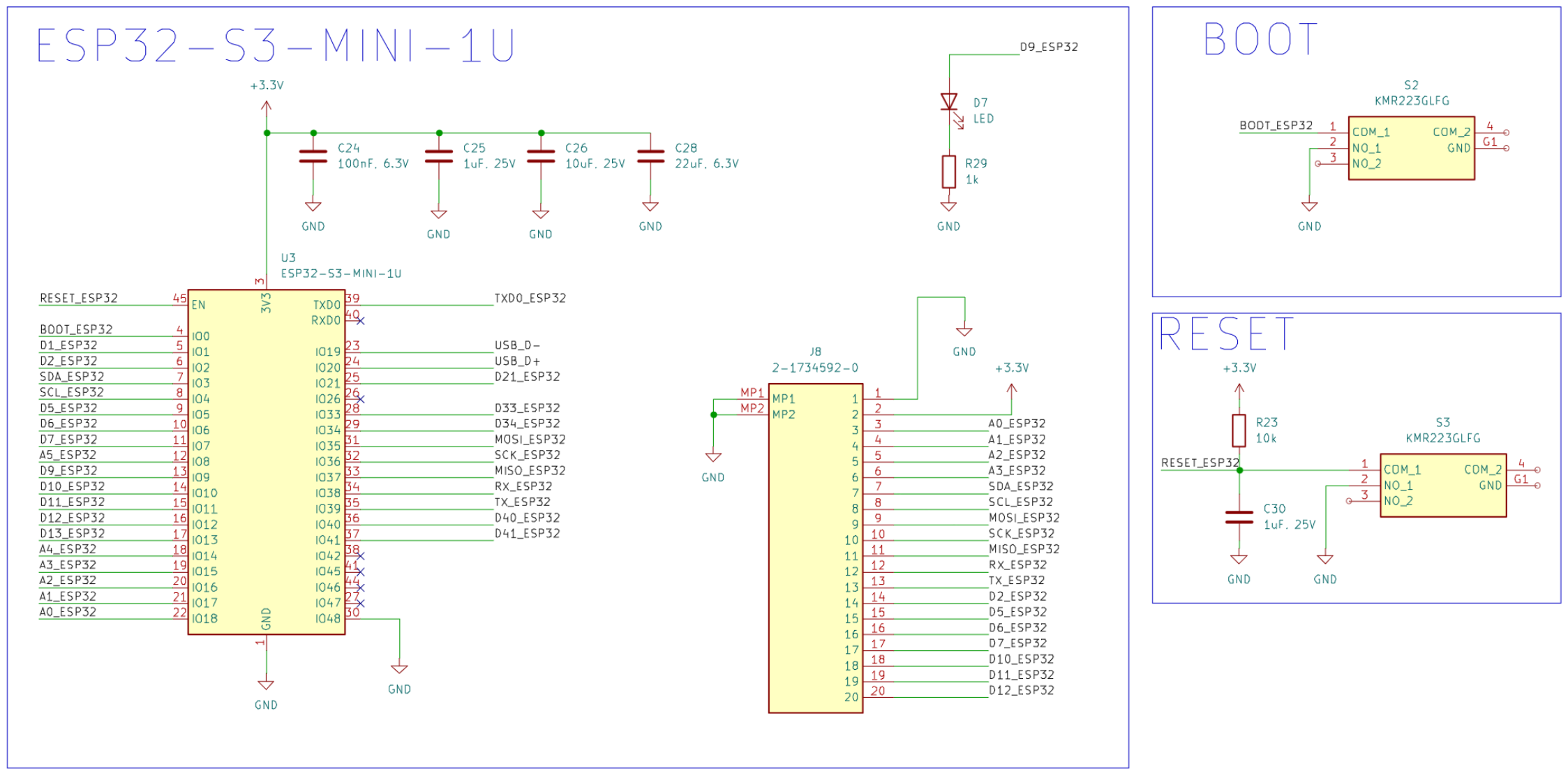
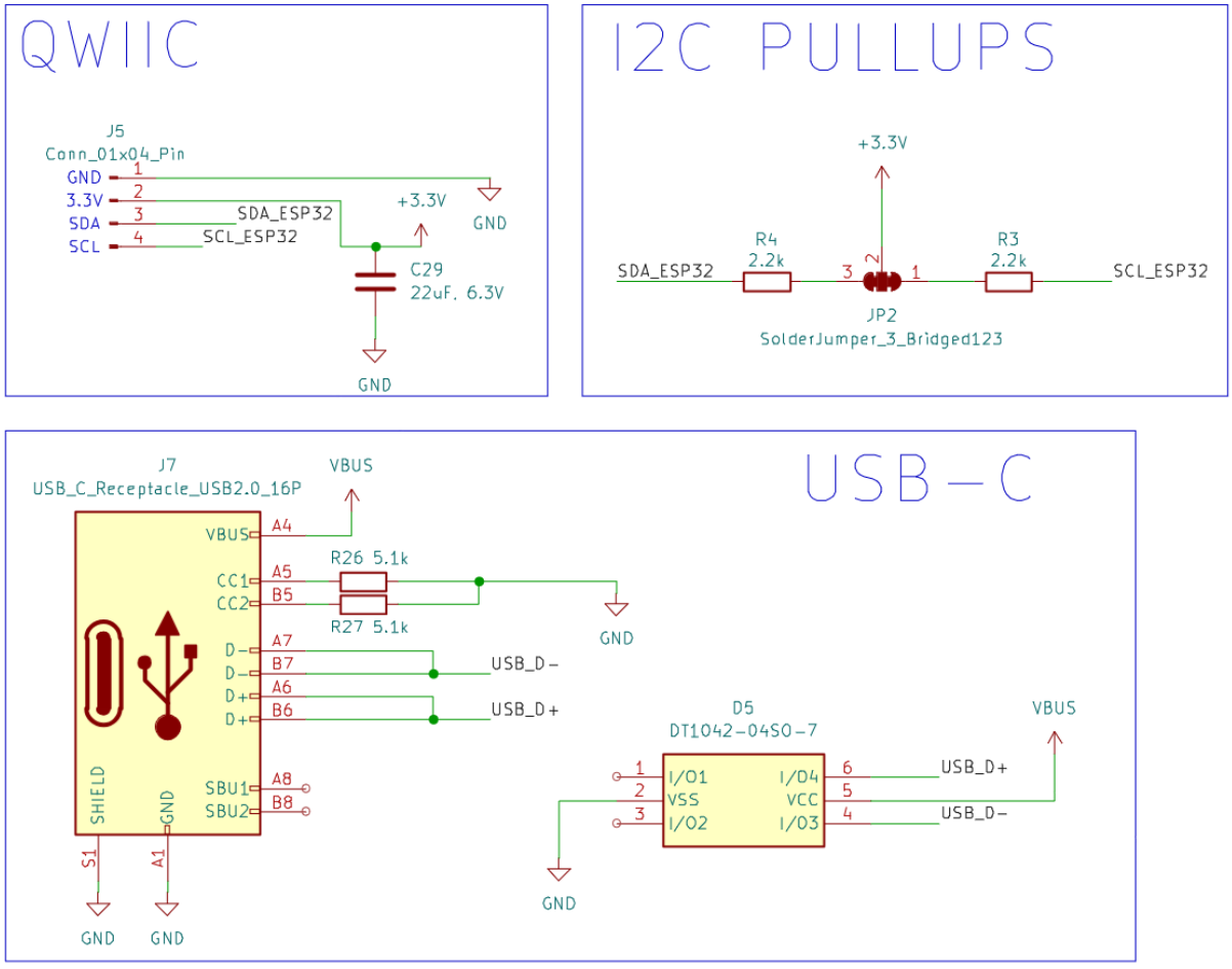
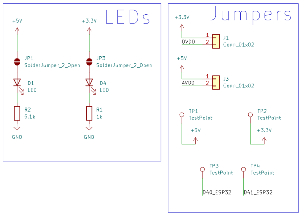
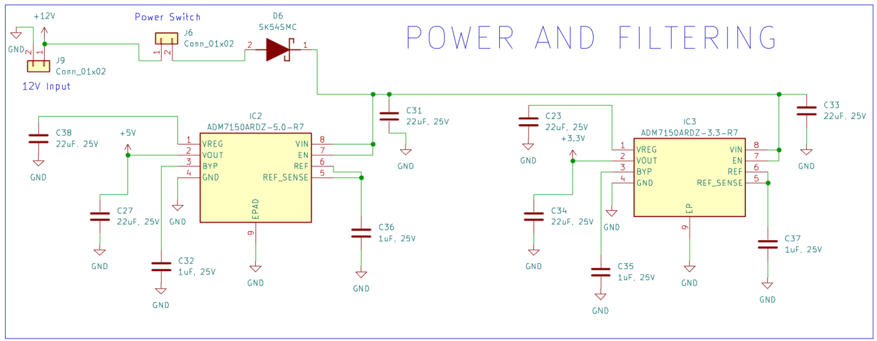
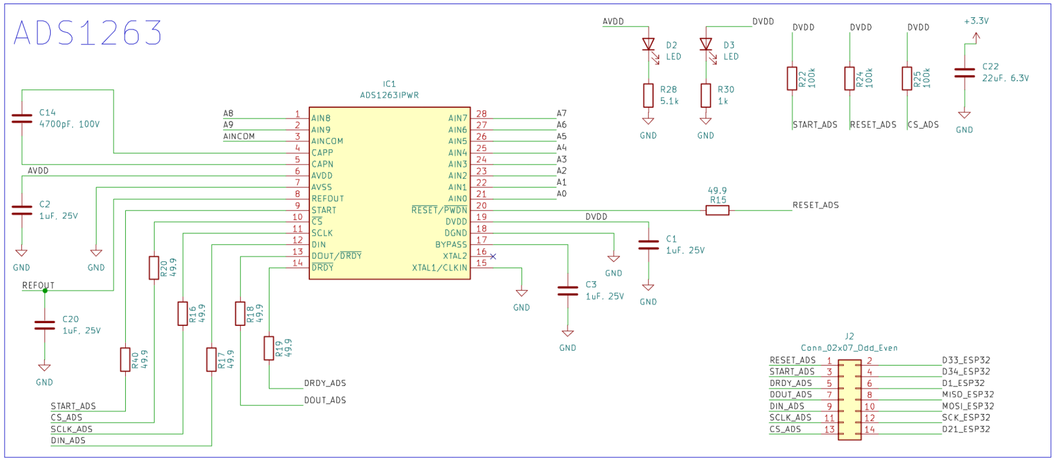
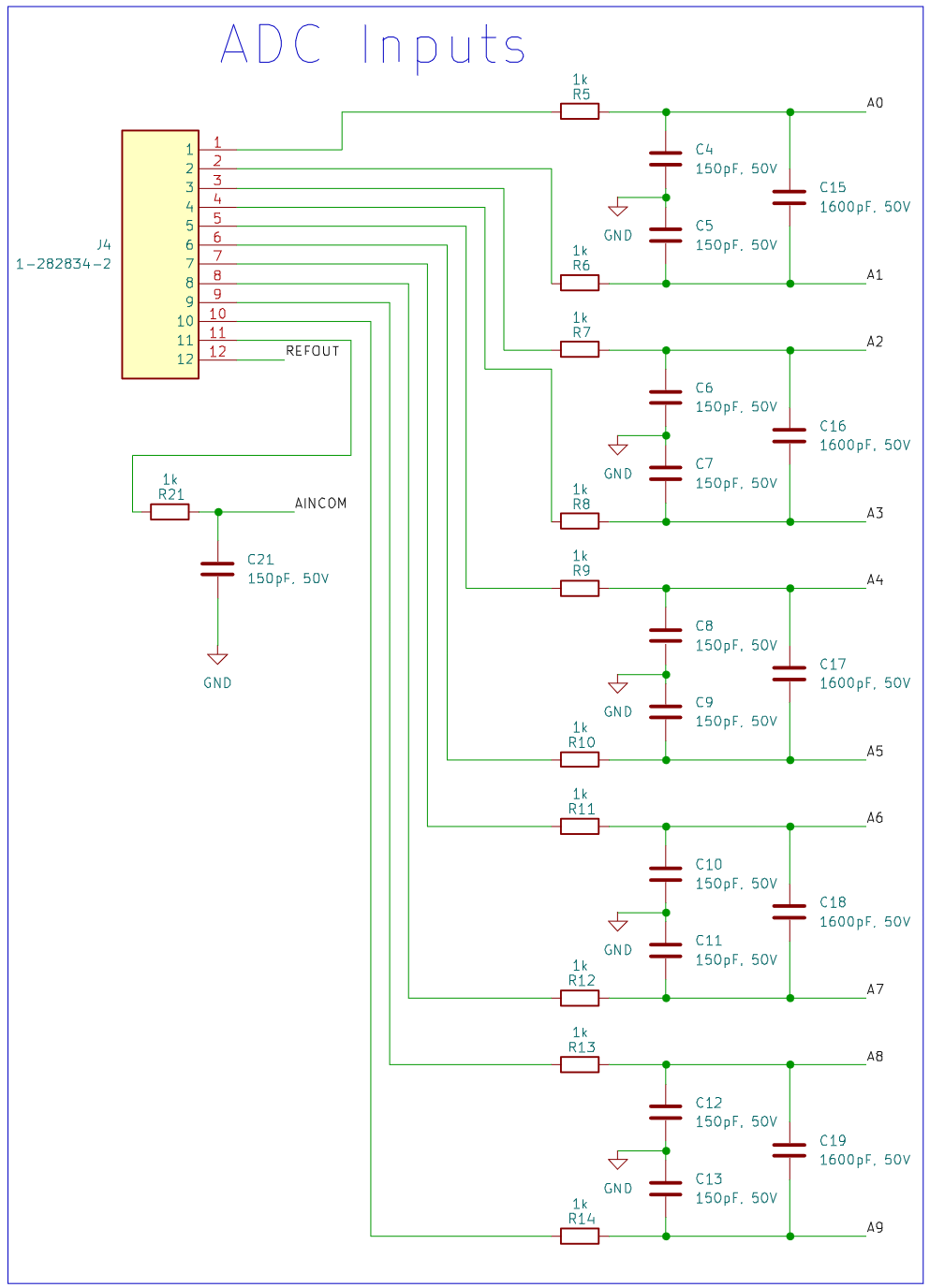
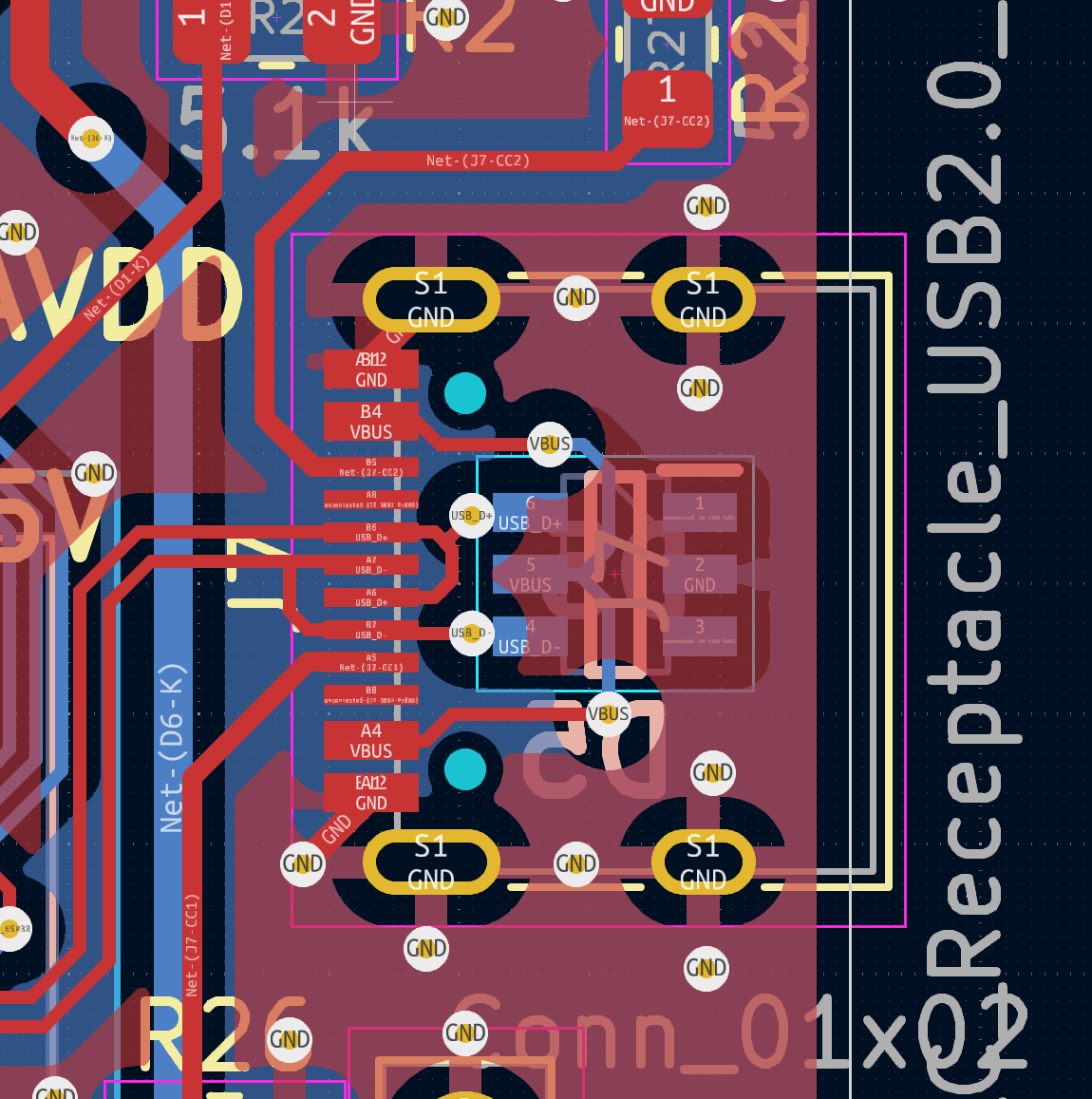
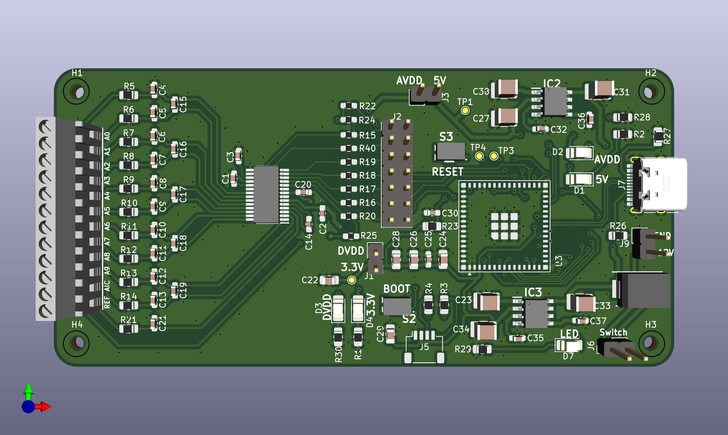
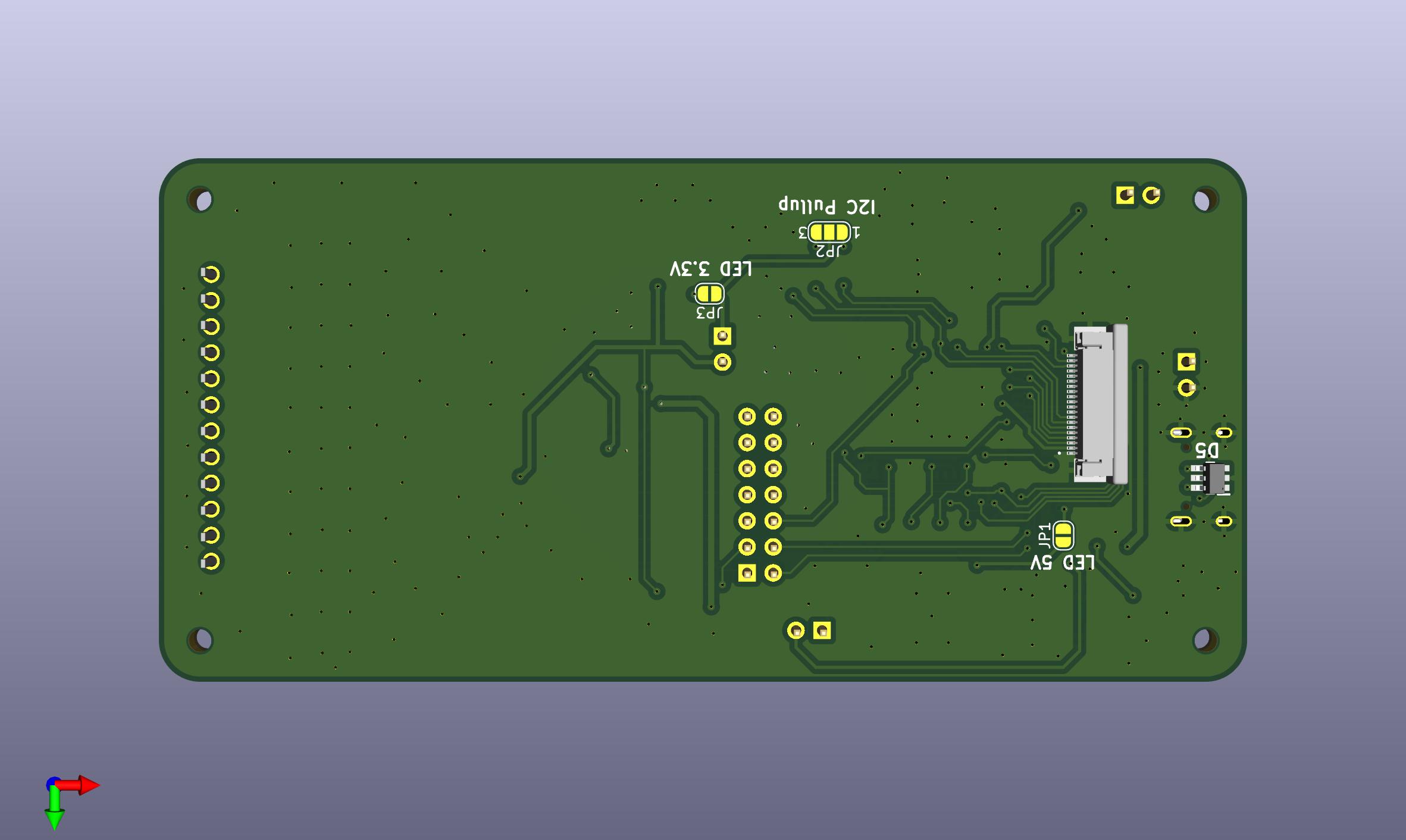
I am designing a four layer PCB with a TI 32-bit ADC (ADS1263) and an ESP32-S3-MINI-1U-N8. The aim is to use this board to read the output of an OPA197, which act as a buffer to a sensing resistor as explained here. I plan to use the JLC04161H-3313 stackup from JLCPCB. The board has also an FPC connector on the bottom side of the PCB to expose GPIO pins of the ESP32-S3. On the bottom side of the PCB, underneath the USB-C connector, there is also a DT1042-04SO ESD protection. I have tried to place the analog part of the ADC as far away as possible from PSU and digital components. The board will be supplied by a 12V input and then there are two voltage regulators (3.3V and 5V) since the ADS1263 needs also a 5V supply at the AVDD pin. The schematic and layout of the ADC part is inspired from TI eval board. The pins in J2 component would normally be connected via jumpers. I placed this in order to be able to connect the ADC to an external MCU or other GPIO pins in case I need to debug or test. Jumpers J1 and J3 are used to enable/disable power supply to the ADS1263.
Any feedback and criticism is really well appreciated and I have some questions:
- Do you see anything wrong that I am doing in the schematic? Any tips for improvements?
- What do you think about the placement I did for the ESD protection? Do you have better suggestions?
- What do you think regarding the two LDOs (3.3V and 5V)? They are quite expensive but I have chosen them for their good PSRR.
- Is the ESP32-S3-MINI-1U-N8 a good MCU for this purpose? It doesn´t have PSRAM built-in. Would you recommend to add external PSRAM for this application?
I place below some screenshot of the schematic and of the PCB's 3D view. I can add more pictures if requested.

