7
\$\begingroup\$

Background: I'm a software engineer with only a little knowledge of circuits--all informal--trying to build an 8-bit sum-carry binary calculator from basic logic gates.

Question: Are there well-known circuits for making a button press (after debouncing) only trigger a signal for exactly one clock cycle while it's being pressed? What are they called so I can learn more about them?

Context: I've got "1", "0", "+", and "clear" buttons on my calculator, but when I press them, I only want the output of this circuit to stay active for a single, but complete, clock cycle (I can't just let it stay high since the clock may oscillate thousands of times while I'm holding the button down, and each tick would be treated as another button press). Basically 1-press = 1 "active" tick. Note that this is after debouncing the button.

So far I've got this circuit, which seems to be working in Logisim:

schematic

simulate this circuit – Schematic created using CircuitLab

Treat the switch as already debounced and the LED on the right as "output". Is this the right way to approach this problem? Or am I completely reinventing the wheel? This sounds like a monostable multivibrator problem, but all of the examples that I've seen of those use RC circuits, and send pulses rather than high signals in-time with a clock...

\$\endgroup\$
3
  • \$\begingroup\$ I wonder how you came up with that quirky DFF/JKFF design with two logic feedback paths. Its strange and interesting, especially if it works. Check my answer for an alternative solution. At the least, you should add a synchronizer to the input signal. \$\endgroup\$ Commented Jul 31, 2013 at 6:56
  • \$\begingroup\$ This is literally one of three different crazy designs I came up with using a variety of flip-flops (most of which with two feedback loops). This is what happens when you have literally no basis on which to start and use a single FF for both logic and synchronization (although, in fairness, it did actually work on both accounts, minus the rare metastability issue you highlighted below). \$\endgroup\$
    – 0x24a537r9
    Commented Jul 31, 2013 at 9:12
  • \$\begingroup\$ I wish there were more questions like this: well thought out and well presented digital logic brain teasers. It certainly is a whacky design. Its looks like the result of mashing components together until they do what you want them to. The FFs in your design do not achieve proper CDC synchronization. Both of them are fed asynchronous inputs so either of them may go metastable. \$\endgroup\$ Commented Jul 31, 2013 at 12:00

1 Answer 1

8
\$\begingroup\$

Here is a digital domain solution. There is not a name for a component that fits the function you describe, but you can use a synchronizer together with a finite state machine.

schematic

simulate this circuit – Schematic created using CircuitLab

Synchronizer

First, your finger is not synchronized to the clock, so the button is assumed to be an asynchronous signal. If the input changes close to the clock it could violate setup or hold time requirements of the DFF0. This can cause the output of DFF0 to be unpredictable (metastable), even a non-logical level. A DFF going metastable is kind of like a coin landing on its side when you flip it. It should be 0 or 1 but actually, in rare cases, it isn't.

The problem is not that the DFF will latch a new value 1 cycle early or late, the problem is that the output may glitch back and forth before stabilizing on a particular value. This could be bad downstream of the design. In this case, our FSM may output a glitch or a pulse that is two clock cycles, for example. The probability that metastability will happen is usually quite low and depends on your DFF, operating clock speed, supply voltage, random noise, and the precise time you push the button.

This problem is called a clock domain crossing (CDC) and requires a synchronization technique. A popular approach is just two DFFs like above. This adds a latency of two clock cycles to the input signal, but this delay is trivial in your application. The synchronizer doesn't eliminate the problem entirely, but makes it an extremely low possibility. Errors due to not addressing a CDC are notoriously difficult to debug. You may pass 1000 tests and fail test 1001. This can lead to painstaking tracing and debugging to try to find the source of the very rare error.

If what you are building has a low tolerance for errors, you should use a synchronizer. You can use the one like above, or use one with three DFFs for even lower probability of failure. Otherwise, if you can tolerate an occasional error, you can get away with just two DFFs and an AND gate for your entire design.

The level of robustness in design should match your application. If you are building a mission critical circuit like a rocket guidance system, you probably should use a 3 DFF synchronizer. If you are building a consumer product with high reliability, go with the 2 DFF synchronizer. If its for a McDonald's happy meal toy, just use a single DFF. A good electrical engineer should be aware of the MTBF requirements for the design, and calculate the probability of failure allowable for the button circuit, the actual failure rate of the synchronizer choices, and choose accordingly.

Finite State Machine

What you want for your pulse generator is actually a finite state machine. Whether you are a complete beginner or a seasoned pro, starting with a state diagram is always recommended.

We start in state A. When the input switches to 1, we want the output, \$ y[n] \$, to be 1. One clock cycle later, \$ y[n] \$ should return to 0, so we need to change the state to B to remember not to output 1. Then we wait for \$ a[n] \$ to be 0 before the state returns to A. From there we start from the beginning. With input signal now synchronized as \$ a[n] \$, we can draw the diagram based on what we want.
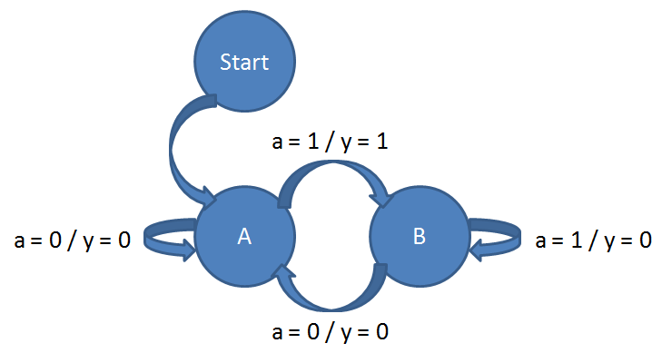
enter image description here

From there you should be able to go from the state diagram to a state table, and then to a FSM circuit. You just need one DFF in your FSM to represent the two states. In the above example, A state and B state represent Q = 1 and Q = 0 respectively, but you can get an equally valid alternative FSM by switching the two states. If it isn't obvious how to get to the FSM circuit, follow some simple FSM tutorials until you get the hang of it.

The output of the FSM above will be \$a[n] \cdot \overline{a[n-1]}\$. This means you only output a 1-cycle pulse when there is a 0-to-1 transition in the input signal.

One final note is that if you can't tolerate errors during start up, you will need to add a reset to your three DFFs. Otherwise, the design above is guaranteed to stabilize to the correct output after three clock cycles after power on.

\$\endgroup\$
7
  • \$\begingroup\$ Duuuuuuude. That is exactly what I was looking for. The problem with my design (although it was functional) was that it merged the two components into one with a backward loop (which was how I "got" a[n-1]) making things unnecessarily complex. My only question, though: why is the middle DFF needed? In my head, I don't really see the purpose. And I tried simulating it without the middle DFF--it seemed to work fine hooking its Q and QN straight to the first DFF. \$\endgroup\$
    – 0x24a537r9
    Commented Jul 31, 2013 at 7:20
  • \$\begingroup\$ Sure, I understand the need for clock syncro (my original circuit had two FFs for just that purpose). And this does sound like a familiar problem. So am I correct that you're addressing the following two-rising-edge-triggered-FF-setup? 1. The user sets the input high right as the clock goes high. 2. The first FF goes (internally) high just in time, although, after the gate delays involved, the clock is now low (at least to the other FF). 3. The other FF sees the clock as low and ignores the output from the first FF. I can see how that would be a problem and the second FF solves it. \$\endgroup\$
    – 0x24a537r9
    Commented Jul 31, 2013 at 8:45
  • \$\begingroup\$ That said, is that kind of metastability condition actually a problem for this particular circuit? I'm trying to minimize parts, and I don't think so. Although I can certainly understand why using two FFs is good-practice for generic circuits, in this particular instance, since we can reasonably rely on a button-press lasting longer than a clock tick (even for a pretty slow clock), won't that erroneous metastability be solved by the next tick? I think as long as we don't accidentally send two high signals, we can afford to drop one if it's eventually sent with the next tick. \$\endgroup\$
    – 0x24a537r9
    Commented Jul 31, 2013 at 8:51
  • \$\begingroup\$ @ox24a537r9, I added a ton of detail to the answer, so it should answer all your questions. I thought the original answer was rather like poof here's a magic circuit that works, so I wanted to explain it so you can see how to do what I did. \$\endgroup\$ Commented Aug 1, 2013 at 3:49
  • 1
    \$\begingroup\$ That's awesome. So much good stuff--especially with the metastability explanation. Thanks! \$\endgroup\$
    – 0x24a537r9
    Commented Aug 1, 2013 at 4:33

Your Answer

By clicking “Post Your Answer”, you agree to our terms of service and acknowledge you have read our privacy policy.

Not the answer you're looking for? Browse other questions tagged or ask your own question.