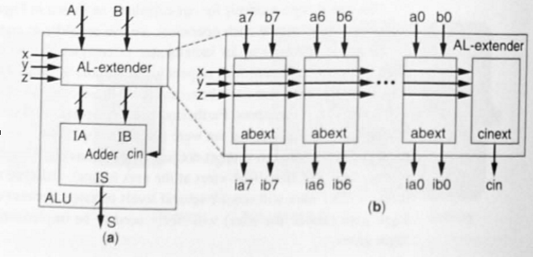
Hey, I'm trying to implement a 4bit ALU based on this 8bit alu design. The ALU has 8 different operations, given by an input of X Y Z
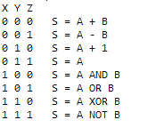
The 8 operations are
 (edit: the last one is just A not, made a typo)
I'm pretty lost as to how to start on the abext. I've determined I need two muxes, one for A and one for B, encoded as either " 0 = Pass A/B, or 1 = Preform a logical operation". However, I'm totally lost as to how to implement each logical operation according to the input of XYZ. I tried to make a 2 input decoder that takes Y, Z and enables "and" gates that are paired with the output of the decoder and the output of each mux, all connected to an or, however that only gives me one output, and I need two.
I'm really just not sure how to create an ALU that demands these requirements, I've never made a normal 4 operation ALU, let alone one with 8 operations. What I'd really like is a a nudge in the right direction in the form of some components I might need to achieve the ia and ib output. Or an example of a similar ALU, as I haven't been able to find one on the internet, and my textbook does not explain the implementation of the abext.
I think for the A mux the selector is X, and for the B mux the selector is X or'd with inv Y. That's all I've tried. Really stuck, would appreciate some help.
(Progress Edit 1) So with the help given below, I arrived at this solution to the abext schematic. Its a little messy, as I'm not the best at organizing these things, but it gets the job done!
https://i.sstatic.net/TJEfd.png
What I've done is for input a, created a 4 to 1 mux paired with a 2 to 1 mux, the 4 to 1 mux has its selectors as Y and Z, and the 2 to 1 has it's selector as X. If x is low, we just take the raw input of a, otherwise we take a logical operation.
For b, we I used two 2 to 1 mux, the first mux takes the input b and b not, this is for addition and subtraction. It's selector is Z. The other mux takes the input of the first mux, and 0. If X' and Y' are both low, it takes the input of the first mux, otherwise it's 0.
Off to hopefully finish the rest of this thing!
(Progress edit 2)
And I'm finished! The rest of the design follows pretty much exactly to the diagram, but here's my implementation of the logic for CIN incase anyone is interested in that. https://i.sstatic.net/fgJw5.png
