4
\$\begingroup\$

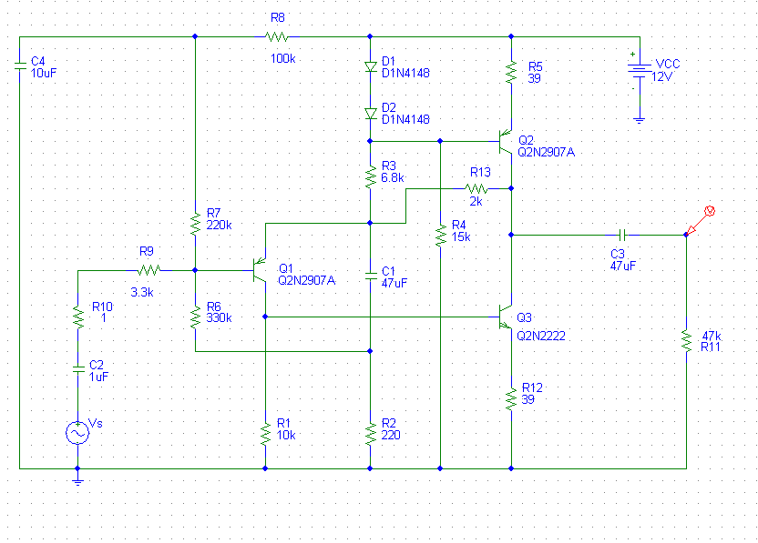
Out of curiosity, I implemented the following headphone amp:

http://www.circuitstoday.com/few-transistor-amplifier-circuits#headphone

enter image description here

I used the exact same components (yes, even the 2N2222/2907 are the nice metal-can ones), checked all connections several times, but the amp just doesn't work. I'm using a bench power supply at 12V, as recommended, and I'm driving a 180 ohm headphones. The amplifier outputs something, but it is very quiet, the gain is less than 0.01. Practically unusable. Also I tried simulating the circuit in Falstad's online simulator, where it shows basically the same thing. The same circuit is available in a few other sites, so it's probably drawn correctly.

One thing I noticed is that if I turn the supply voltage down, the gain actually increases, to the point that at 6 VDC it's almost unity gain, but with heavy distortion. There's almost no distortion at low levels (e.g., if I'm turning the pot to 1/10), but the distortion is unbearable at any usable gain levels.

After some tweaking in the simulator, I simply removed the biasing diodes D1 and D2 - and voilà - the amp works perfectly. It amplifies around 10x, and the distortion is gone.

Now, what I'm asking here is why are these diodes required, what kind of biasing is this? It is obvious that they do serve a purpose - without them, Q2 goes into saturation, and is basically bypassed - the amplification is done by Q3 alone. Without them, the current through Q2 and Q3 increases several times - at 12 V it is almost 100 mA and the transistors get quite hot (it's bearable at 9V though). The original circuit hints at 15 mA current. Is it possible that the original circuit designer made an error in the specification of the diodes? How can the circuit be "fixed" to adhere to its original idea?

I'm not very adept in analogue circuits, and biasing in particular, so some explanation of why the circuit was designed that way would help a lot.

EDIT: here's a link to the simulation. You can click the switch near the diodes to see what happens.

\$\endgroup\$

2 Answers 2

4
\$\begingroup\$

Assuming, for quick analysis sake, that the diodes and emitter-base junction each have 0.7V across, this leaves 0.7V across R5. The emitter current for Q2 is then:

$$I_{E2} \approx \dfrac{0.7V}{39 \Omega} = 18mA$$

Thus, the first thing you should is check to see if you do in fact have this. Measure the voltage across the R5 and use Ohm's law to calculate \$I_{E2}\$. If it is "in the ballpark", the bias circuit is working as designed.

without them, Q2 goes into saturation, and is basically bypassed - the amplification is done by Q3 alone

Q2 isn't configured as an amplifier in this circuit, it is an active load (current source) for Q3. Note that the voltage at the base of Q2 is effectively constant while the audio signal from Q1 is applied to the base of Q3.

Essentially, Q2 supplies an approximately constant current "down" out of the collector.


I've simulated this circuit with pSpice and it doesn't work well at all which doesn't surprise me for a number reasons. The output stage is highly non-linear but there's no DC or AC feedback around it. The collector voltage of Q3 is thus poorly controlled.

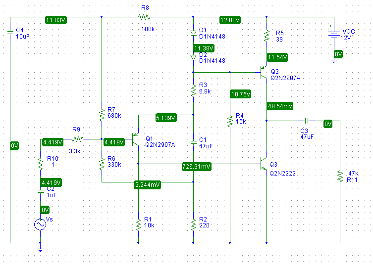
In fact, when I simulate the operating point, I find that Q3 is in saturation.

enter image description here


To simply address some of the problems with this circuit, I added two resistors:

  • An emitter resistor for Q3 to add local feedback
  • A resistor between the collector of Q3 and the emitter of Q1 to provide both DC feedback, to set Q3's collector voltage at about 6V, and AC feedback to set the open-circuit small-signal gain to about 20dB.

enter image description here

By adding these resistors, I need to change the value of R7 to 220k. The values I picked for the added resistors and R7 are not necessarily optimum and were found by "playing around" with the values and simulating until I got what I wanted.

A more rigorous derivation of the gain and operating point dependence on these resistor values would be fun but I honestly don't have the time at this moment but... maybe later.

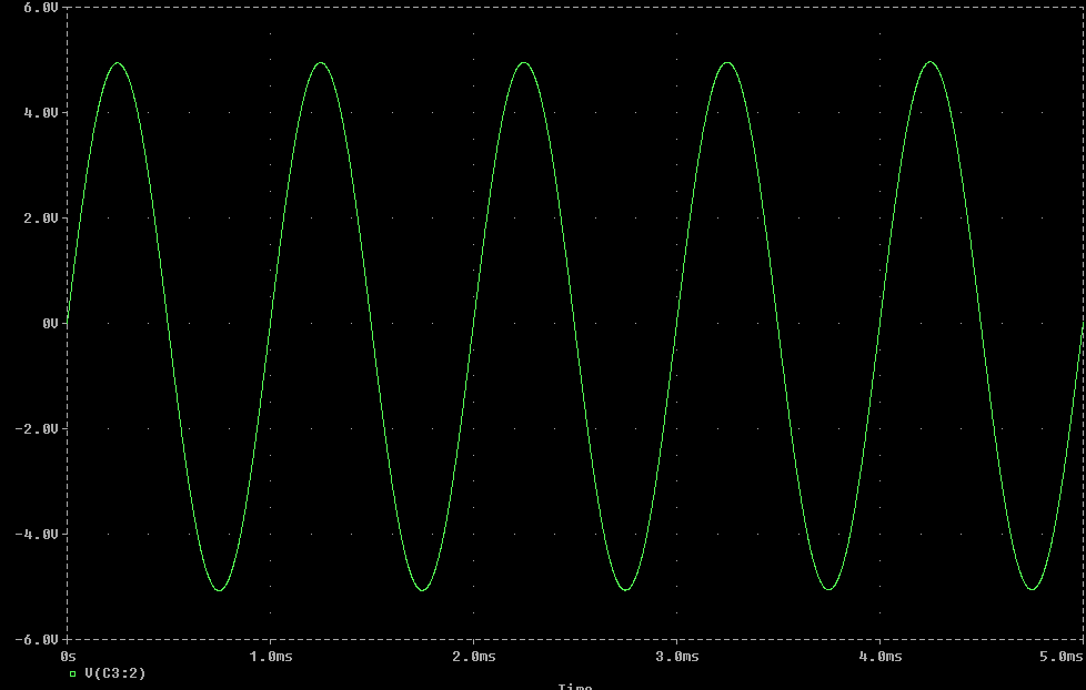
Below is a transient simulation with 1Vpp 1kHz input:

enter image description here

\$\endgroup\$
4
  • \$\begingroup\$ You can make it work (ish) in simulation by tweaking R1 down to bring Q3 out of saturation, around 2-3k it starts putting most of the waveform through. \$\endgroup\$
    – pjc50
    Commented Dec 4, 2013 at 14:56
  • \$\begingroup\$ @pjc50, the problem is that the operating point will still be unstable since there is no DC feedback. The output stage has very high gain that is dependent on temperature and beta. \$\endgroup\$ Commented Dec 4, 2013 at 15:40
  • \$\begingroup\$ This answers my question completely, thanks a lot! I'll just add the modifications you suggested and the next time will research the circuit (in a simulator) thoroughly, before jumping straight to implementation :) \$\endgroup\$
    – anrieff
    Commented Dec 4, 2013 at 18:54
  • \$\begingroup\$ @anrieff, be aware that with 180 ohm headphones, the amplifier will clip at about +2V. This is a consequence the fact that Q2 is operating as a 12mA current source and so, the maximum voltage is about (12ma) (180 ohms) = 2.2V. (However, Q3 can "pull" more current since it is not current limited. Thus, the negative clipping level will be more around -5V or so.) So, for sinusoidal signals, the maximum average power into 180 ohms without clipping will be about 11mW. \$\endgroup\$ Commented Dec 4, 2013 at 19:35
1
\$\begingroup\$

The two diodes are meant to be a rough voltage source. As long as current is kept flowing thru them, which it seems is the case, they will hold the base of Q2 two diode drops below the power rail. The B-E junction of Q2 is also a diode drop, so that leaves one diode drop accross R5. Let's say that is 700 mV accross 39 Ω, which means the current is about 18 mA. In other words, D1, D2, Q2, and R5 make a roughly constant 18 mA current source.

Note that R4 is a constant current drain thru the diodes so that they stay at roughly fixed voltage, and R4 also provides the base current fo Q2 to operate.

The output voltage is controlled by how much current Q3 draws. Theoretically, if it draws less than 18 mA, its output will go high. If it tries to draw more than 18 mA, its output will go low and only 18 mA will be drawn. For a perfect current source, this circuit would have infinite gain.

The amazingly bad part of this circuit is that there is no feedback at all that tries to keep the output at roughly mid voltage. Any slight change in biasing or gain or phase of the moon can change the delicate balance. Q3 doesn't even have a emitter resistor, so the current it draws will be highly unpredictable.

Basically, this cicruit is crap. A low side drive working against a current source is a legitimate topology for low power levels, but this implementation is just plain junk.

There are a number of ways this mess could be fixed. The most obvious would be using the node between Q2 and Q3 as a feedback input to the first stage. If done right, this would control the gain, which would flatten it over the intended frequency range, and it would actively control the DC bias point to near the middle.

\$\endgroup\$
1
  • \$\begingroup\$ Yep, while you were adding your answer, I was adding two resistors to the circuit, to "patch it up", and simulating. Another problem with this circuit is high output impedance. I assume it's meant to drive high-impedance headphones only. \$\endgroup\$ Commented Dec 4, 2013 at 15:19

Your Answer

By clicking “Post Your Answer”, you agree to our terms of service and acknowledge you have read our privacy policy.

Not the answer you're looking for? Browse other questions tagged or ask your own question.