36
\$\begingroup\$

How do I interface 3.3 V Input/Output to 5 V Output/Input? I need it primarily for an Arduino Due but any general purpose bidirectional circuit (or IC) would work.

Some people advised me to use the SN74AHC125 and CD4050 ICs, but I don't understand how they work or how to interface with them.

\$\endgroup\$
10
  • 2
    \$\begingroup\$ What is the intended frequency range? \$\endgroup\$
    – alexan_e
    Commented Jan 28, 2014 at 8:51
  • 1
    \$\begingroup\$ For example assume I want to connect 5V device to a 3.3V arduino. I couldn't figure out where to connect the 5V output and the 3.3V input. And what about output a 3.3V from an arduino for example to a 5V device ? What do you mean by frequency range ? \$\endgroup\$
    – 3bdalla
    Commented Jan 28, 2014 at 8:59
  • 1
    \$\begingroup\$ I'm not sure that I got your point, I haven't dealt with frequencies before, my purpose is for simple electronics :| \$\endgroup\$
    – 3bdalla
    Commented Jan 28, 2014 at 9:15
  • 3
    \$\begingroup\$ sparkfun has a board, its called a 'level converter' \$\endgroup\$ Commented Jan 28, 2014 at 10:48
  • 1
    \$\begingroup\$ Usually I used ICs from texas instruments. TXS and TXB series have bidirectional voltage translators (e.g. TXS0102 have two channels) \$\endgroup\$
    – frarugi87
    Commented Dec 1, 2015 at 17:50

9 Answers 9

49
\$\begingroup\$

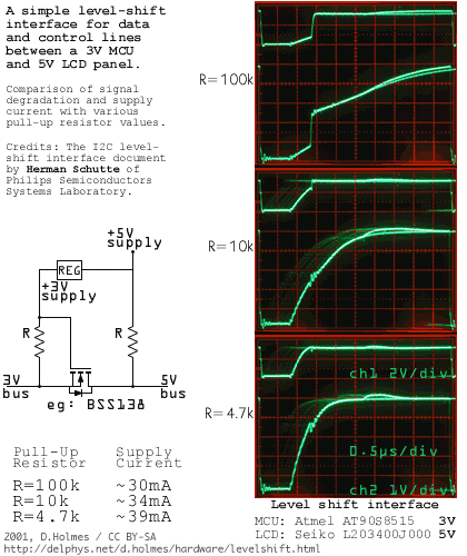
A very simple bidirectional level translator can be made with a single N-mosfet:

enter image description here

The mosfet used should be a model with a low Vgs threshold, so that it can have a relatively low Rds-ON (ON resistance) at the intended input voltage level (3.3v in this case).
BSS138 in one such example, it has a Vgs-th of 1.5v max and is specified to have a low drain-source resistance with Vgs voltages as low as 2.5v (maybe slightly lower too).

The shown example uses 3.3v <-> 5v translation but it can also work with 2.5v <-> 3.3v or 2.5v <-> 5v, even between 2.5v <-> 12v. The range is only limited by the characteristics of the mosfet used.

The shown circuit is based on an application note from NXP
AN97055 Bi-directional level shifter for I2C-bus and other systems
New shorter version: AN10441 Level shifting techniques in I2C-bus design

When L1 is high (3v3) or floating R1 keeps the mosfet off so R2 pulls the drain side high (to 5v).

When L1 is pulled low then the mosfet conducts and the drain becomes low.

When a low level (0) is applied to H1 then that voltage is transferred through the substrate diode to the source side (L1)

Please note that the resistance size can affect the speed (image source)

enter image description here

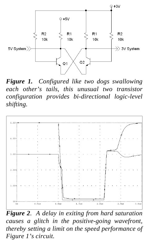
Alternative transistor solution enter image description here


Relevant articles you may find useful:

\$\endgroup\$
0
14
\$\begingroup\$

Since the question seems oriented towards an IC that provides bidirectional level shifting, consider the Texas Instruments TXB010x family of parts: TXB0102 has 2 channels, TXB0104 has 4 channels, and TXB0108 has 8 channels.

The stand-out feature of this family of ICs is that signal direction is automatically sensed, so a separate direction setting pin is not needed.

Switching speeds up to 10 MHz work reliably. The theoretical maximum speed may be higher - the datasheets are not explicit about this from what I can determine.

I have a TXB0108 working between a 3.6 Volt MSP430 Launchpad and a 5 Volt Arduino Nano, so the use case of the question is covered.

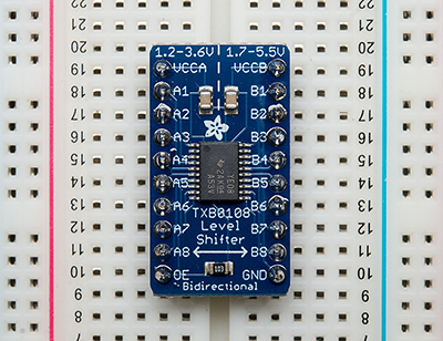
For the purposes of trying it out, Adafruit offers a prebuilt module incorporating the TXB0108, which saves you the trouble of soldering an SMD part. There may be similar options for the 0102 and 0104 from them or others.

8-channel Bi-directional Logic Level Converter - TXB0108

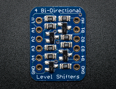
If the intent is to level-shift an I2C signal, which isn't ideally suited to the TXB series ICs, an option that specifically addresses the pull-up resistor and open collector topology of I2C is a module like this, again sold by Adafruit and other vendors.

I2C level shifter

This module uses BSS138 MOSFETs in the way described in the answer by alexan_e. While it is not a single IC such as the question asks for, it perhaps fulfills the intended purpose. Alternatively, it is simple to build this circuit yourself using MOSFETs.

\$\endgroup\$
2
  • \$\begingroup\$ +1 Nice find! ... Your link to TXB0102 is actually to the TXS0102. I haven't determined the difference, but this is noted in the datasheet of the TXS0102: "Its primary target application use is for interfacing with open-drain drivers on the data I/Os such as I2C or 1-wire, where the data is bidirectional and no control signal is available. The TXS0102 can also be used in applications where a push-pull driver is connected to the data I/Os, but the TXB0102 might be a better option for such push-pull applications." Here is the actual link to TXB0102 \$\endgroup\$
    – Tut
    Commented Jan 30, 2014 at 12:17
  • \$\begingroup\$ @Tut Oops, slip-up, thanks. My own needs are met by the TXB0108, so the others are more of a "nice to know" for me. :-) \$\endgroup\$ Commented Jan 30, 2014 at 12:49
11
\$\begingroup\$

Another thing you should consider is whether you actually need level shifting at all. Many chips have 5V tolerant input pins even when running at a voltage lower such as 3.3. The atmega CPU also interprets anything above 0.6*Vcc or 3V for an arduino as a logic high, so a 3.3V signal can directly drive an arduino pin with no level shifting.

Assuming you are using a 5V arduino and need to talk to a 3.3V part, if the part has 5V tolerant inputs (many do nowadays), just connect em up and it will work. If your bidirectional line is an open collector design, such as i2c where the devices only pull the line low then just attach the pull up resistors to 3.3V instead of 5V and things will just work.

Otherwise all you need to do is make sure the line doesn't go above 3.3V, you can do that with a resistor and zener, put a resistor on the arduino line then a zener to clamp the voltage to 3.3V. zener resistor clamp
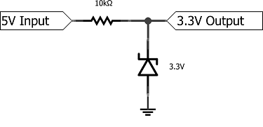
(source: repetae.net)

You may be tempted to live dangerously and just use the 10k resistor and nothing else. The reason this (sometimes!) works is that there is a clamping diode inside the recieving chip that shunts excess voltage to vcc or 3.3V. This diode will burn out if you try to pull the entire 3.3V line up to 5V through it (in addition to whatever damage caused by pulling that line to 5V), however with the resistor not much current will flow and assuming your 3.3V line has a non-trivial load on it it won't change the level of your power line substantially but there are lots of caveats. So, in general, don't do this unless you have a local, isolated 3.3V bus and really can't spare the extra two cents for the zener. I only mention it because you will see it in schematics for dirt cheap breakout boards you get on ebay and might be tempted to copy it, just don't let it sneak past the breadboard into a production design. :)

Edit just noticed you were using the newer 3.3V arduino, so just invert what I said above, the zener resistor trick will still work although apparently some of the i/o lines on the due may be 5v tolerant, there seems to be some disagreement on the forums. The teensy 3.1 is also a nice little ARM board that has all 5V tolerant pins and is less than half the cost of the due and better designed IMHO http://www.pjrc.com/store/teensy31.html

\$\endgroup\$
3
\$\begingroup\$

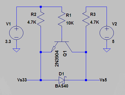
From the cheap[er?] solution department, the FET (from the accepted answer based on the NXP appnote) can be replaced with a BJT and Schottky diode as in Silicon Labs AN883. Their schematic is a bit complicated with other things, so I've extracted the essential bit here and reoriented it so it looks like in the accepted answer for easy comparison of the two schematics:

enter image description here

The BJT does translation in the low->high direction only... exactly as discussed in Single transistor level up shifter. The Schottky replaces the body diode of the FET for the high->low translation.

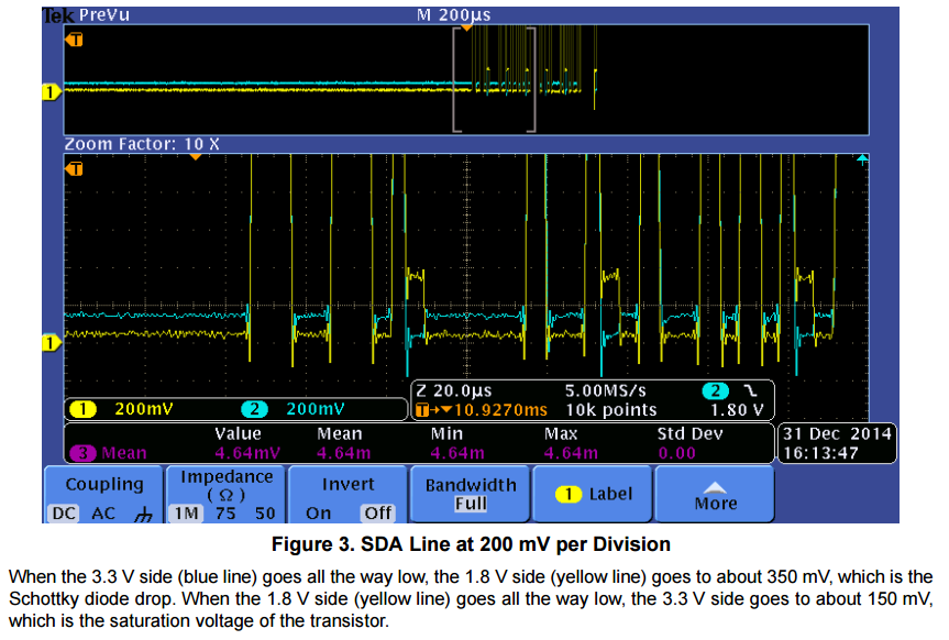
Below is their zoomed in scope measurement for a 3.3<->1.8V translator; they also propose this schematic for 5<->1.8V translation etc. When doing 3.3<->1.8V translation a MMBT3904 had only 150mV (saturation) drop. The BAS40 diode had 350mV drop in the opposite direction. These offesets affect (obviously) the logic-low level output on the low and respectively high side of the translator.

enter image description here

They had nice CMOS devices on both sides, so input impedance wasn't much of an issue. There was no visible degradation/offset of the logic-high margins in their 1V/div trace, so I haven't bothered including it here. The input impedance of their devices were at least 1Mohm from what I can tell from a simulation. Logic-high margins start to degrade below 100K input impedance or so.

Also, they recommend this BJT-based translator only up to 300KHz or so.

I'm not sure which of these solutions is cheaper in practice, FET or Schottky + BJT... but this one certainly needs more parts... unless you use one of those diode+transistor packages, which do exist, e.g. PZMT1101. But you also need 3 resistors.

\$\endgroup\$
10
  • \$\begingroup\$ What is the expected current draw/power consumption of this method in comparison to the FET-based method? \$\endgroup\$
    – KyranF
    Commented Dec 1, 2015 at 18:04
  • \$\begingroup\$ @KyranF: I haven't compared them, but if you're worried about that either is going be not rosy because of the pull-ups. The low power CMOS versions look like m.eet.com/media/1103155/Fig2.gif That's from eetimes.com/document.asp?doc_id=1231111 which is good article comparing various approaches. \$\endgroup\$ Commented Dec 1, 2015 at 18:08
  • \$\begingroup\$ Thanks for the links. I suspect the BJT approach would be very high power in comparison during the times when the base is saturated. The constant load of pull up resistors is indeed worrying for any design, especially battery operated designs. \$\endgroup\$
    – KyranF
    Commented Dec 1, 2015 at 18:11
  • \$\begingroup\$ @KyranF: I've looked at it in simulation: the transistor and the diode dissipate uW of power while the resistors dissipate mW. Actually the BJT dissipates around 100uW, the diode 1uW. FET or BJT won't matter here... resistors having path to ground for static dissipation is what matters. This is with 1Meg input impedances. \$\endgroup\$ Commented Dec 1, 2015 at 19:04
  • \$\begingroup\$ @KyranF: I tried using ON's BSS138LT1 model, but that gives negative average power disspation in LTspice (of -63uW)... so I think their model may be problematic. Garbage in... garbage out. Also it started to oscillate (at much higher frequency than the signal) when driven from the high side. It's a subckt model rather than simple MOS model, so it's hard to figure out what's going on. [continued] \$\endgroup\$ Commented Dec 1, 2015 at 19:42
2
\$\begingroup\$

Well, there are many. You need to specify what is your maximum frequency, how many bits you need, etc. In short, you can use any voltage level translator IC. Texas Instruments has a neat selection tool for the very same purpose: http://www.ti.com/logic/docs/translationresults.tsp?sectionId=458&voltageIn=5.0&searchDirection=2&voltageOut=3.3#voltintf

\$\endgroup\$
2
\$\begingroup\$

You can find a nice summary of all methods here

http://playground.arduino.cc/Main/I2CBi-directionalLevelShifter

\$\endgroup\$
2
\$\begingroup\$

Also, if you are looking for a great electrical isolation as well as bidirectional level shifting functionality, I would recommend ISO1541. It is fairly cheap and provides good protection through isolation.

\$\endgroup\$
1
\$\begingroup\$

The most simple solution is to run all your circuits at 3.3V. HC chips will happily run at that level.

When that is not possible, you can make things much more simple when you restrict yourself to one direction. A HCT chip at 5V will accept 3.3V levels just fine, and a simple two-resistor divider can reduce 5V to 3.3V. Some uC are 5V tolerant on their pins, so you don't need the divider. And if you put 5V pullups on the pins, and switch between ground and open (=input), you have a passable 0-5V output.

For coupling open-collector busses (I2C, dallas 1-wire) the BS138 trick is a way to go. There are small chips for I2C that put the two FETs in one housing. (PCA9306 etc.)

But if you really want bi-drection level translation: such chips do exist, check for instance TXB0108.

\$\endgroup\$
-4
\$\begingroup\$

A simple solution is using the SN74LVC244AN. Can be powered with 3V3 and is 5V tollerant on the inputs.

\$\endgroup\$
2
  • 5
    \$\begingroup\$ That's not bidirectional. \$\endgroup\$
    – Matt Young
    Commented Jan 21, 2016 at 21:41
  • \$\begingroup\$ No but the 74LVC4245 is. \$\endgroup\$
    – Bregalad
    Commented Feb 28, 2019 at 16:03

Your Answer

By clicking “Post Your Answer”, you agree to our terms of service and acknowledge you have read our privacy policy.

Not the answer you're looking for? Browse other questions tagged or ask your own question.