0
\$\begingroup\$

I was studying sequential circuits and I am at the very infant stages of the course. After studying the D flipflop I realized that the purpose was to let the data line change the output if clk=1 or keep the data same if clk=0. The circuit that is generally used is derived out of the SR latch which is a complex circuit using two feedbacks. Why cant I use a simple one feedback MUX circuit with the following boolean function?

Q(n+1)=Qn.C*+D.C
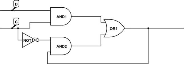
schematic

simulate this circuit – Schematic created using CircuitLab

The circuit diagram at the gate level would be as shown above, where D is the data line and C is the Clock. Am I being dumb somewhere??

\$\endgroup\$

2 Answers 2

1
\$\begingroup\$

Assuming that your circuit works, and I'm not going to bother to find out, it isn't a fundamentally different circuit from an SR latch. You've removed the !Q output, so one of the feedback paths in the latch now looks like a feed-forward path. This seems intuitively true because you have shifted the OR gate to the right, so the path from the bottom AND gate to the OR gate doesn't look like a feedback path anymore.

In any event, the important characteristic is not the number of feedback paths but the number of gates. You replaced a nice 2-gate latch with four gates, so most people would say you've taken a step backwards. Worse, the natural gate style in CMOS is NOR and NAND rather than OR and AND so your solution might actually require additional inverters for a practical implementation.

\$\endgroup\$
3
  • \$\begingroup\$ Yup, I read up a lot about it over the net and they also seem to be of the same NAND/ NOR opinion. (Although the no. of gates used are still lower. A latch uses 2 gates, but this circuit implements the entire FlipFlop. The FlipFlop needs 4 gates, all of them NAND. I've worked with only 3) I dont understand why NAND and NOR have to be the basic Dig IC styles although. Thanks anyways...:) \$\endgroup\$
    – Ghosal_C
    Commented Feb 12, 2014 at 14:51
  • 1
    \$\begingroup\$ No, your circuit is not a flip-flop, at least not how I define that term. A flip-flop is an edge-triggered storage element while a latch is a level-sensitive storage element. Your circuit is a level-sensitive D-latch. The signal you have called C is a latch-enable signal, not a true clock. \$\endgroup\$
    – Joe Hass
    Commented Feb 12, 2014 at 22:09
  • \$\begingroup\$ Okay. Maybe you are right, maybe it's just a gated latch, but some books define it as a flip-flop too, but I see you have experience in the matter, so probably your nomenclature is more pure. Joe, you seem to be a really helpful man and you have some sturdy experience too, could you suggest me some book or reading which would help me cover topics right from digital gate design (comb and seq.) all the way through microprocessors to instruction set architectures. I have an exam coming up in about 6 months. I will also have to go through a project of creating a 16B prog machine and define its ISA \$\endgroup\$
    – Ghosal_C
    Commented Feb 13, 2014 at 7:24
1
\$\begingroup\$

Your circuit is not balanced. Path delay for clock signal to reach AND1 and AND2 is different. Therefore clock signal will reach the inputs of two AND gates at different time. Hence if circuit is driven by high speed clock there may a case where clock drives both AND gates at the same time.

\$\endgroup\$
2
  • \$\begingroup\$ Okay, I was wondering how the design for data latches evolved? I am new to studying digital design and every circuit that I have studied has a background logical approach, but for SR latches/ D-latches, there is no background evolutionary logic given. As soon as I started sequential logic, I was handed out a design of an SR latch and I was shown that on application of different inputs the output simply satisfy the necessities of a latch, but the circuit just appeared out of nowhere. No, logic simplification, no K-Map, nothing...Can u give me an idea??? \$\endgroup\$
    – Ghosal_C
    Commented Feb 20, 2014 at 14:36
  • \$\begingroup\$ SR latch is the simplest possible design. Since it is basic building block of memory elements no design is involved. But D latch is implemented from SR latch by using a not gate between S and R inputs. \$\endgroup\$ Commented Feb 20, 2014 at 15:31

Your Answer

By clicking “Post Your Answer”, you agree to our terms of service and acknowledge you have read our privacy policy.

Not the answer you're looking for? Browse other questions tagged or ask your own question.