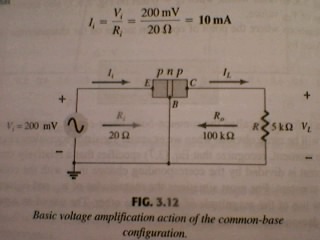
I am reading "Electronic Devices and Circuit Theory" by Louis Nashelsky, Robert L. Boylestad.
I am not able to grasp article 3.5: Transistor Amplifying Action. I've mention some particular points on which I am having questions. In general I want to understand this article. I want to understand what the authors are saying here.
At the last of the article the authors say that "because the source current is transferred from a low- to a high-resistance circuit, that's why we call this device as transfer+resister \$\rightarrow\$transister." But I don't understand the way they reached this statement. I've bought this book and I don't want to waste my money; I do not want to put this book aside and buy some other book. Please help me understand it.
The circuit schematic is as shown:

- Input resistance \$R_i= 20Ω\$,
- Output resistance \$R_o = 100KΩ\$.
- Input voltage \$V_i = 200mV\$
- The emitter current \$I_i= V_i/R_i = 10mA\$
Since \$α_{ac}≈1\$, so \$I_c≈I_e\$
Output voltage \$V_L=I_LR=(10mA)(5KΩ)=50V\$.
Voltage amplification is \$A_v=V_L/V_i=50V/200mV=250\$.
What I don't understand is:
What is \$200mV\$, is it the instantaneous voltage, rms voltage or peak voltage? What are \$I_L ,\ I_i,\ R_o\$ and \$R_i\$ etc's?
Why the input resistance doesn't get affected by the load resistance. In fact, what determines the input resistance? Are the \$n\$ region and load resistance acting as a set of two parallel resisters for \$V_{in}\$?
Since there is no DC biasing i.e \$Vcc\$ is \$0\$, how is this high output voltage supplied?
How can we apply KVL to the loop BCB? The power dissipated across \$R\$ is \$I_LV_L=0.5W\$. What is the source of this high power, is it the minute reverse bias collector junction (which is quite impossible because a P-N junction cannot provide energy)?
This circuit acts like a current source. \$I_L\$ is completely independent of the load resistance. How can we use this (common base) circuit as an amplifier for low resistance load? Or suppose we want to apply the \$V_L\$ to some resistor of order 10 ohms, the output will reduce to \$10 \Omega \times 10mA = 100mV \$ so the output voltage is reduced than the input voltage(200mV).
If the biasings are suppressed please explain this circuit. That is with proper biasing at the same parameters and how much \$V_{EE}\$ and \$V_{CC}\$ should have been applied? what are the actual input and output waveforms?
