3
\$\begingroup\$

I'm trying to climb the Cadence learning curve, coming from an Eagle background.

My board is four-layer, with a ground plane underneath the top layer. I have a surface mount IC that has an exposed pad, which should be soldered to ground. I want to avoid putting vias in this pad. Since two edges are free of pins, I am trying to pour a copper region larger then the opening in the solder mask, and then I'll put the vias there, connecting it to the ground plane.

Here is the part:
enter image description here

In Eagle, I would pour the polygon and assign it the same net name as the exposed pad. The two areas would merge nicely.

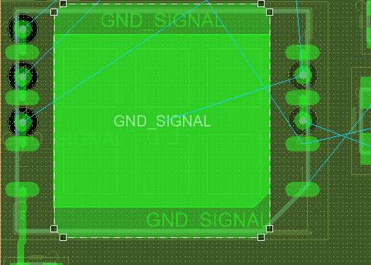
I have done this in Cadence, using a dynamic copper fill, on the top layer, and assigning the same net name ("GND_SIGNAL"). The two areas do not connect, and I get a trace between the two "floating" areas, connecting them to the exposed pad:
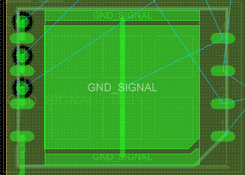
enter image description here

I suspect that this may be thermal relief between the pad and the pour. Is there a method to force Cadence to NOT use thermal reliefs, on just this one pad? I've looked over the docs, and asked google, but I'm not finding an answer.

Of course, it may be something else completely. Does anybody know how to do this?

\$\endgroup\$

3 Answers 3

7
\$\begingroup\$

I finally called Cadence support, and they were very helpful! Maybe there's a good reason to pay for their Maintenance Contract :) This answer is for PCB Designer 16.6. I don't know if it will be the same for earlier versions...

There are two methods to suppress thermals: the Global method, and the Instance method. The instance method only affects a single (dynamic copper) shape.

Since thermal reliefs are generally helpful, I don't want to turn them off globally. The Instance method, on the other hand, is just what I was looking for.

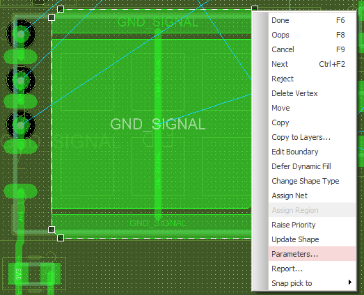
To set up the parameters for a specific instance, select the shape, then right-click. Choose "Parameters..."

RightClick

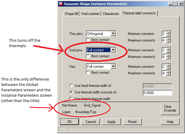
Or, if you prefer a global change, click on Shape > Global Dynamic Params. Either way, it brings up the same window. (you'd better remember which path you took to get there...)

parameters

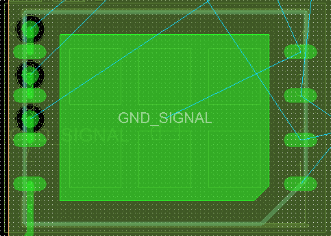
Go to the "Thermal relief connects" tab. Under Smd Pins, choose "Full Contact". Perfect!

Result

Take care everyone. Happy Engineering :)

\$\endgroup\$
3
\$\begingroup\$

Is there a method to force Cadence to NOT use thermal reliefs, on just this one pad [or just some selected pads] ?

I had the same question for a while, and I couldn't find a proper way to do this: neither for old OrCAD 10.5, nor for newer versions.

My workaround is to put a copper area (in addition to the copper pour) over the thermal pads. Unlike a copper pour, a copper area doesn't isolate tracks and doesn't have thermal relief. The copper area is connected to the same net as the thermal pad and copper pour. Copper area is larger than the thermal relief.

P.S. Hopefully that there is a better way of doing this. I'll keep an eye on this thread.

\$\endgroup\$
8
  • \$\begingroup\$ That's how I'd do it - overlap stuff with copper. \$\endgroup\$
    – Andy aka
    Commented Apr 1, 2014 at 7:31
  • \$\begingroup\$ Thanks Nick, @Andyaka. I got the answer from Cadence :) Please take a look! \$\endgroup\$
    – bitsmack
    Commented Apr 1, 2014 at 22:36
  • \$\begingroup\$ +1, Nick, what's the difference between copper area and copper pour? 10x. \$\endgroup\$ Commented Dec 23, 2016 at 16:12
  • \$\begingroup\$ @Sergei Copper area is just a polygon filled with copper. If a copper area covers a trace, then it will paint over the trace. If there are multiple traces covered by a copper area, then the copper area will paint over all of them and short them. \$\endgroup\$ Commented Dec 23, 2016 at 16:47
  • \$\begingroup\$ @Sergei Copper pour isolates tracks that cross it. Copper pour may also be attached to a net. In that case, it will isolate all nets, except the one that it's attached to. Copper pour has got a more complex behavior. In my experience, copper pour is used more often than copper area. Here's an example of a copper pour in one of my previous questions. Notice how the copper pour had created an isolation gap around the resistors and traces. \$\endgroup\$ Commented Dec 23, 2016 at 16:48
-1
\$\begingroup\$

An old thread, I know, but in case anyone comes across it - the correct answer is DON"T DO THAT! Don't bypass the thermal reliefs. They are there for a reason. When your board goes through the tunnel the part will not stay where you want it to if there is a giant mass of ground plane attached to the thermal pad. The copper will suck out all the heat that is supposed to be melting the solder and making a good joint. The part may float up or twist or just not get soldered at all. A very bad practice. If you are at the very limits of your thermal design (a bad place to be, poor design) and need every ounce of copper to keep your chip from burning up you can: 1. Increase the size of the thermal spokes by changing them in the Constraint Manager. 2. Put in an array of vias to a ground plane in another layer or on the back side or even to a large copper area on an inner layer. If the vias have the minimum hole size or are tented on the bottom side it will prevent the solder from escaping through them. They don't have to be filled. You should do this anyway.

I know all the part manufacturers' example boards and sample designs show massive copper planes right under the pads with no reliefs, but they only do that because it makes the chip look better in the thermal image test. If you want decent yields in production, use a higher power chip, don't run it at the limits and use thermal reliefs. The Contract Manufacturer has spoken.

\$\endgroup\$
2
  • \$\begingroup\$ Old thread. But this is not very good advice. Boards are very often designed this way. If the method of assembly is reflow, it does not create any problem, because the entire board is heated up more or less at the same time. The entire board and all the solder is hot. The part will not move because the solder mask will prevent solder from flowing away from the pad. A large fill does not imply that the solder mask is opened any more than normal. If the part has to be reworked by hand, it can be very difficult. But sometimes you just need to use the PCB as a heatsink to make the design work. \$\endgroup\$
    – user57037
    Commented Aug 11, 2017 at 1:57
  • \$\begingroup\$ I agree, @mkeith. Whether or not we're near a thermal limit, there are good solid reasons to not put vias under pads. If you leave them open, they wick solder from the joint. If you tent them on the top, the mask thickness holds the part away from the copper. If you tent only the bottom, expanding air and/or flux can disturb the joint. The good solution is to put plugged vias in pads, but this increases board cost... \$\endgroup\$
    – bitsmack
    Commented Aug 11, 2017 at 4:59

Your Answer

By clicking “Post Your Answer”, you agree to our terms of service and acknowledge you have read our privacy policy.

Not the answer you're looking for? Browse other questions tagged or ask your own question.