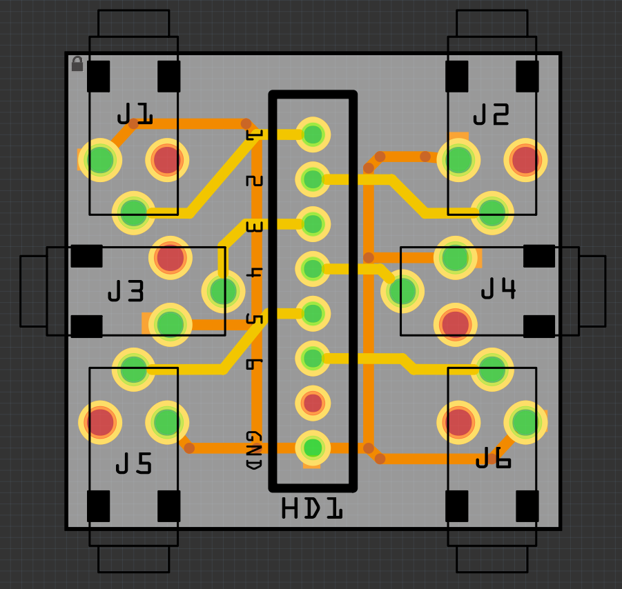
All your GND are already connected together. Thus the question is would a copper fill change anything?
Part of the answer comes from understanding the difference between your routing and one with a copper fill.
A single copper trace can be modeled as a small inductor. It also has some resistive behavior. If you replace your traces by a GND fill, that inductive behavior would be reduced as well as the resistive one. Is this a good thing? Usually yes.
The concept of GND is to have a common reference across the system. The better your GND is, the better your reference is. Thus it's often a good thing to reduce the cause that would create voltage differences in your GND.
Reducing the resistance (DC effect) or inductance (AC effect) would make your GND more "solid" thus better.
But this is not the only thing to consider here. Other factors are:
- Solderability. It's sometimes easier to handsolder thing connected to tracks than things connected to copper planes. Your soldering iron has to heat up the mass of copper of the plan instead of a trace and this makes hand soldering a little bit more tricky.
- EMI. You said that you are using audio jacks but it's not specified if it's for audio signals. In some case e.g. high frequency signals or very nervous signals (fast rise time) you want to keep your return current close to the signal tracks. Having a fills, or better: a full GND plane, is very good at this. This way, the return current which follows the path of least impedance in AC, would be just beneath your signal trace and the current loop formed by the signal and it's return current would have a very small area and thus be more immune to magnetic coupling (noise).
- Short circuits. If you plan to make your board yourself by etching, you may want to avoid to have GND everywhere close to your signal trace. Very small defects would short your signals to GND.
I am sure there are other considerations. But in summary, it should not hurt to use GND fills.

