1
\$\begingroup\$

I am developing a mixed-signal embedded system that requires both 5V and 3V rails.

The 5V rail powers an analogue sensor and a precision ADC. The nature of the sensor is such that its output will be DC most of the time and slow-changing the rest of the time. Low noise and low temperature coefficient are the most important aspects of this rail.

The 3V rail supplies the digital circuitry (ADC digital interface, MCU (SPI & UART comms), modem). There are two SPI slaves - the ADC and a DAC. The noise, tempco and regulation of this rail are not critical. Low cost is most important.

The ADC is continuously sampling, the SPI transactions are periodic and the UART communication is on-demand (and infrequent). The microcontroller's internal oscillator runs at 1MHz and is sync'd to a 32768Hz watch crystal.

There needs to be a wide input voltage range (10 - 40V DC). For this reason I intend to use three series LDOs; the first will connect to the input and will output 5.5V. The reason for 5.5V is that the 5V supply has a dropout voltage of 200mV, which needs to be maintained over a large temperature range.

This 5.5V rail will feed the two other LDOs. Two ways of achieving this are shown in the image below (the 40 ohm resistor is integral to an IC - all circuit current flows through it):
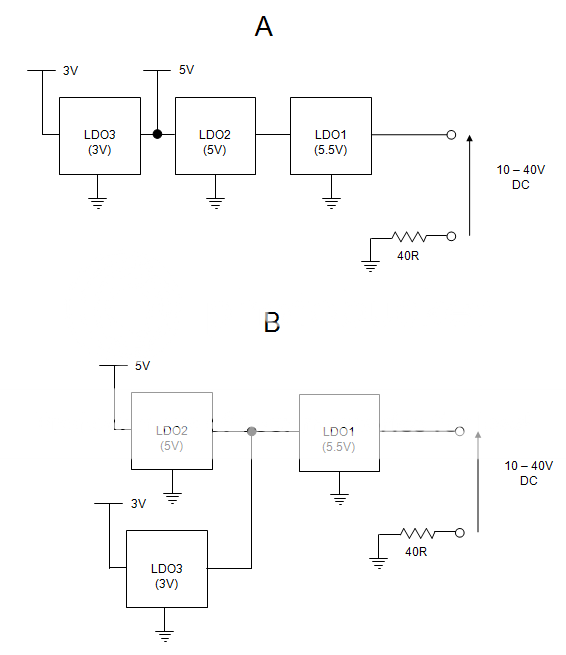
3V and 5V Supply Topologies

With reference to the image, please evaluate the truth of the following statements:

1) Topology B is much superior, even if the supplies are bypassed well, as changes in demand will still have some effect on the 5V rail load regulation.

2) There is not much difference between topologies A and B, if the supplies are well bypassed and the 5V rail has good load regulation.

3) Statements 1) and 2) can't be meaningfully evaluated without more information about the system and components.

4) The greatest effect by far will be due to the grounding scheme (e.g. daisy-chained ground connections back to the 40 ohm resistor as opposed to a star configuration).

5) Both topologies are a strange/inefficient way of achieving the objective. There are solutions that are much better in terms of cost and performance.

6) This question shows a lack of understanding.

EDIT: 7) LDOs are generally better at dealing with line variation than load variation. So while topology B might have more of an effect on the 5.5V rail, the 5V LDO will handle this better than if there was an effect on its load (as there is in topology A).

EDIT: To clarify, the circuit is low power - only 3.1mA in total is drawn from the input.

\$\endgroup\$
7
  • 3
    \$\begingroup\$ A note for others, the diagrams are read from right to left. Not left to right. Threw me off for a second, was thinking "is this guy connection the output of a 5v and 3v LDO together?" \$\endgroup\$
    – Funkyguy
    Jul 10, 2014 at 15:23
  • 1
    \$\begingroup\$ The first regulator, taking the 10 - 40 volts down to 5.5, should be a switching regulator. A linear regulator will waste a great deal of power, and will require a large heatsink, unless the total current requirement is very low. \$\endgroup\$ Jul 10, 2014 at 15:40
  • \$\begingroup\$ 1. What are the 5V and 3.3V current requirements? 2. Can you quantify the 3.3V rail's voltage tolerance, noise, and tempco requirements? 3. With 1Mhz ~ 30.5 * 32768, how does your sync work? \$\endgroup\$
    – EM Fields
    Jul 10, 2014 at 15:44
  • \$\begingroup\$ @ShannonStrutz, Yes that is a bit confusing. I don't know why I drew it that way round. \$\endgroup\$
    – user49118
    Jul 10, 2014 at 15:53
  • \$\begingroup\$ @PeterBennett, this is a two-wire 4-20mA system - output current = supply current = proportional to the measured process. The total current through the 5.5V LDO is 3.1mA, which is the total consumption. The rest goes through a transistor that is not shown on the diagrams. \$\endgroup\$
    – user49118
    Jul 10, 2014 at 15:56

1 Answer 1

0
\$\begingroup\$

B is better- you're not directly injecting digital noise into your precision analog supply.

It might be even better to draw the 3.3V supply directly from the input supply. For example, a single BJT (emitter follower) from the 5.5V regulator will give you a bit under 5V out, which your 3.3V LDO can easily handle (assuming it can't handle 40V directly). That will also reduce the dissipation in the 5.5V LDO (do you really have to call it that close, and do you really need an LDO in this position?).

\$\endgroup\$
5
  • \$\begingroup\$ It doesn't have to be so close to the bone; 6V would probably be more sensible, especially given that the maximum input of the 5V supply is 15V. It doesn't have to be an LDO either. The '5.5V' IC is the LT3014BHV from Linear Technology. One of the reasons I'm using it is because it can survive transients of 100V for 20ms. The product will have lightning protection (from strikes on the power cables). There is a TVS at the input that clamps the input at 91V (standoff voltage is 43V) when subjected to an 8/20us waveform (as per EN 61000-4-5). \$\endgroup\$
    – user49118
    Jul 10, 2014 at 16:20
  • \$\begingroup\$ I'm not worried about the power dissipation, due to the low current demands, but your idea sounds like a good way of improving performance. If I experience any noise issues, then I will give this a try. Thanks. EDIT: The 3V supply definitely can't handle 40V, it's the MCP1702 from Microchip. It has very low cost (~£0.2) and low quiescent current (which is vital). \$\endgroup\$
    – user49118
    Jul 10, 2014 at 16:21
  • \$\begingroup\$ Yes, I thought it looked like a 4-20mA loop-powered system, so the drop in the 40R is only 800mV. Of course the TVS leakage is error, but not much you can do about that. Sometimes a high-voltage depletion-mode MOSFET makes sense as the primary pass device. \$\endgroup\$ Jul 10, 2014 at 16:23
  • 1
    \$\begingroup\$ The TVS leakage current is 0.2uA at 25degC and 1uA at 85degC, which is pretty small compared to the system accuracy, so I'm not too worried about it. \$\endgroup\$
    – user49118
    Jul 10, 2014 at 16:41
  • \$\begingroup\$ The DAC I am using is an integrated 4-20mA IC. It's the IC with the 40R resistor (the voltage across it is one of the inputs to a virtual ground amplifier, whose purpose is to compensate for the changing supply current, which would otherwise appear directly on the output signal). The datasheet says that a BJT should be used instead of a FET for 3 reasons: 1) FETs have large threshold voltages, beyond the range of the driving pin, 2) the higher load capacitance might degrade stabilty, and 3) the driving pin relies on the base current for biasing. \$\endgroup\$
    – user49118
    Jul 10, 2014 at 19:29

Your Answer

By clicking “Post Your Answer”, you agree to our terms of service and acknowledge you have read our privacy policy.