2
\$\begingroup\$

I've noticed, when looking around the internet, that almost every circuit showing the usage of a N-channel MOSFET has the load before the drain, and the source pin is tied to ground.

From what I understand, the following is true:

Vgs is the voltage difference between the Gate and Source that is required to fully turn on the MOSFET, causing it to act like a very low impedance connection between the Drain and Source pins.

I'm assuming the following:

Because of this, it is much simpler to make the source pin ground, and to input at least Vgs to the gate to turn it on.

Is this correct, or is there another reason to have the Source tied to ground?


With that out of the way, I'm trying to build a circuit that will turn on an LED, and provide input to a Raspberry Pi (Max 3.3V input, shown as 'SIG_25%') when 'SENS_25%' is on. 'SENS_25%' being on means anywhere from 50kΩ to 600kΩ between 5V and the MOSFET input. When off, it is open, and the 1MΩ resistor prevents it from floating. The circuit shown currently is able to (not fully) turn on the LED, but the output at 'SIG_25%' is too low to be detected by the Raspberry Pi (Tested at 0.44V).

I believe the reason that this doesn't work as intended is that the MOSFET in the circuit (IRF530N, the only one I had laying around) has a too high Vgs value (2V min, 4V max), and the input is too low for it (When 'SENS_25%' was 470kΩ, the gate was measured at 3.39V), turning the MOSFET into a somewhat large-value resistor across the drain & source.

I want to know, if I find and use a MOSFET that has a maximum Vgs of less than 3V, would my circuit work?

The LED in the circuit is just a plain old color LED, Vf of ~1.8V, 20mA optimum current.

I cannot place the 'SIG_25%' above the MOSFET, as when the MOSFET is turned fully off, I measure 4V there, which both makes the signal useless (It would always be on), and it is too high for the Raspberry Pi to handle safely. This is also why I placed R2 at the Source pin, as I couldn't think of a better way to do this.

Here is the circuit I've currently got:

Current Circuit Diagram

\$\endgroup\$
7
  • \$\begingroup\$ What are you referring to when you say "When 'SENS_25%' was 470kΩ"? Do you mean when R1 was such a value? What is the input voltage at the mosfet gate? \$\endgroup\$
    – sherrellbc
    Commented Jul 10, 2014 at 19:43
  • \$\begingroup\$ I stated that 'SENS_25%' would act like a resistor with anything between 50kΩ to 600kΩ between 5V and the gate when on, and open when off. I tested the MOSFET by putting a 470kΩ resistor between 5V and the gate, as this would be similar to actual conditions. \$\endgroup\$
    – CaiB
    Commented Jul 10, 2014 at 19:48
  • \$\begingroup\$ So the driving circuit has those output characteristics? That means the gate of the mosfet only sees whatever the output of the divider would be using those values (i.e. 4.76V to 3.13V). Or did I miss again? \$\endgroup\$
    – sherrellbc
    Commented Jul 10, 2014 at 19:54
  • \$\begingroup\$ And you're only driving the LED with just over 1mA of current, so very little is dropped across the diode, little across the resistor, and most across the mosfet. What is the gate voltage as measured by a multimeter? \$\endgroup\$
    – sherrellbc
    Commented Jul 10, 2014 at 19:57
  • \$\begingroup\$ Yes, you got this correct. The MOSFET would see a resistor between 5V and its gate, or nothing at all. Also your numbers (4.76V to 3.13V) are correct. \$\endgroup\$
    – CaiB
    Commented Jul 10, 2014 at 20:01

2 Answers 2

4
\$\begingroup\$

With 1 meg from the gate of Q1 to GND, and SENS25% at 50k, Q1's Vgs will be 4.76 V, while with SENS25% at 600k, Vgs will be 3.125V.

That means that Q1 is almost certainly capable of being fully turned on - albeit somewhat slowly - by SENS25%, but R2 will prevent that from happening because the higher Vgs goes, the higher the current through R2 goes, which will cause the voltage dropped across it to increase, raising the voltage on the source, partially defeating the rise in Vgs.

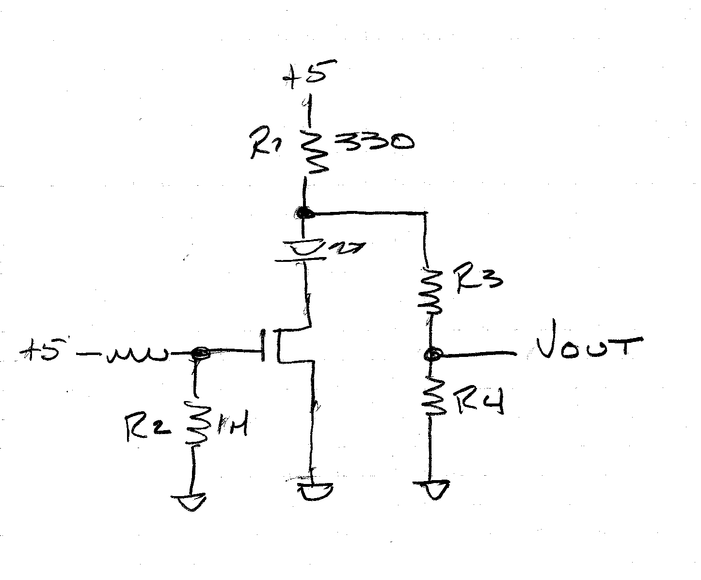
A solution might be to wire your circuit like this:

enter image description here

Where, when Q1 is OFF, 5V across R1 R3 R4 will make Vout equal to a "1" into your Raspberry Pi, and when Q1 is ON, the drop across the LED and Q1's Rds(on) will make Vout equal to a "0".

If not, I think you'll need some extra circuitry or a different way to go about it.

\$\endgroup\$
1
  • \$\begingroup\$ I'll mark your answer as the accepted one, as I used information from it, and based my design on yours. Thank you! \$\endgroup\$
    – CaiB
    Commented Jul 21, 2014 at 22:39
2
\$\begingroup\$

The reason a MOSFET Source or BJT Emitter is connected to ground usually is simply due to the advantages of that topology. The common-source or common-emitter topology allow for extremely high voltage gain compared to other topologies. See here and here for more info on that.


Your use-case isn't any different in needing/wanting very high current/voltage gain. You want to turn at a minimum 8.3uA (5V/600kohm) into a usable logic signal.

The circuit I describe should work much better than your original circuit because of the immediate amplification of the signal followed by a voltage level shifter all packaged into one vertical path from Vdd to ground.

If you use a BJT, you'll likely want to use a darlington pair for higher gain. A MOSFET may be used in place of the BJT.

Once the Mosfet or BJT/Darlington pair has performed your current/voltage amplification, you want to ensure the output voltage is below 3.3V and above the switching voltage for the GPIO pin of the Raspberry pi. That's accomplished here with the LED and diode shifting the ON-voltage down to 5V-1.8-Vd. R3 is a current limiting resistor to prevent LED burnout and what the output voltage will be dropping across. Make sure R4 is a very high resistance element because otherwise, the PNP base voltage will never be high enough to shut itself off.

Lastly, keep in mind that all resistance values there are ballpark values and are likely not optimal. D3 may not be necessary depending on the tolerance and value you're after. It could also be replaced with a small resistance to create a voltage divider between it and R3.

schematic

simulate this circuit – Schematic created using CircuitLab


NOTE: If you're really stuck on using an NPN or an NMOS, your topology will work, you just won't have as clean (slower, less precise voltage) a turn-on/off. What you need to do is make your R1 a higher value. As it stands, you've got a voltage divider with 5*1e6/(1e6+6e5) = 3.125V. If you swap your LED and resistor, your LED voltage drop is 1.8 V you said, so you'll need to have the input signal > Vt+1.8. As it stands you would need your voltage divider give you 4+1.8=5.8V. You'll want a very low threshold NMOS and you'll likely want to increase your voltage divider voltage by increasing R1.

If you don't swap the LED and resistor, you'll be pinning your output voltage when it's on at input voltage divider - Vt. The problem here is that your input voltage will vary a lot due to your input resistance varying between 50k and 600k so your voltage output "pinning" will vary a lot and not be terribly pinned to a precise value. This is all due to it being a common-drain topology (also known as a source-follower because the source follows the voltage of the gate).

\$\endgroup\$

Your Answer

By clicking “Post Your Answer”, you agree to our terms of service and acknowledge you have read our privacy policy.

Not the answer you're looking for? Browse other questions tagged or ask your own question.