9
\$\begingroup\$

I am trying to route the SPI between MCU and ADC. However, the pin orders between MCU and ADC are not matched, there are crossings. A four-layer board is used.(signal - ground - power - signal)

I tend not to use vias (I am not familiar with grounding, EMI and etc.), as the SPI runs at 50MHz. I have the impression that a via from one signal layer to the other will worsen the ground loop. Is the impression correct?

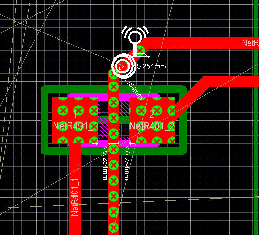
Therefore, the following connection is used: A resistor acts as a bridge... The resistor is serial connected for matching purpose. Is this kind of connection valid? I dont like it as well, since the resistors are in 0402 package, which makes the trace through very thin. enter image description here
And

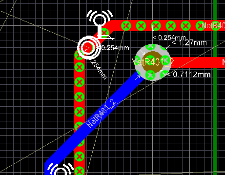
One last question, should I worry the interference between different signal traces, if the following connection is used (with vias)? enter image description here

EDIT

What my question actually is:

This post mentions something similar, PCB routing: EMI and signal integrity, return current questions

It says:

"The second component is a high frequency return signal which tries to follow the signal trace on the ground plane. If you switch layers from say the top layer through to the bottom layer on a 4 layer board (signal, ground, power, signal) the HF return signal will as I understand it try to jump from the ground plane to the power plane by detouring through nearest available path (nearest decoupling cap, hopefully... which to HF might as well be a short)."

How is the power plane influenced? And why is that??

It should also be related with this post: The best stack-up possible with a four-layer PCB?

The first point of the first answer:

1.Signal layers are adjacent to ground planes. Stop thinking about ground planes, and think more about reference planes. A signal running over a reference plane, whose voltage happens to be at VCC will still return over that reference plane. So the argument that somehow having your signal run over GND and not VCC is better is basically invalid.

\$\endgroup\$
1
  • \$\begingroup\$ These days a viable solution would be: use a better MCU, where the pins can be assigned with more freedom :) \$\endgroup\$ Commented Mar 10, 2022 at 16:46

3 Answers 3

14
\$\begingroup\$

SPI bus at 50MHz can easily run a couple of inches thru a few vias without hitch. Wavelength of 50MHz is 6 metres but realistically because fast edges are used you need to think ten times faster. Even so that's a wavelength of 60 cm. Rule of thumb is keep tracks smaller than a half of a quarter wavelength (other folk will use other rules of course) and this means 7.5 cm or 3 inches.

Try and keep clock and data same length and if you hit problems on long stretches you might have to terminate at high frequencies with 10pF in series with 100 ohm (more likely on clock than data).

There is no great theory in my answer, just a whiff of theory and some experiences and he odd rule of thumb. Bottom line - use a ground plane - it's no excuse to say you are not familiar with grounding - get familar - it'll be the difference between something always working and something nearly always never working - it's that big a deal.

\$\endgroup\$
9
  • 1
    \$\begingroup\$ Agree totally. I made a small mistake in ground plane at 10MHz and 1.8V - I accidentally created a loop - and was rewarded by the most unpleasant coupling behaviour from a nearby USB cable. Had to bin the PCB and redo it. It is indeed that big a deal. \$\endgroup\$
    – carveone
    Commented Jul 14, 2014 at 10:16
  • 1
    \$\begingroup\$ @carveone Could you please explain how your loop was created? Through an answer with some pictures? It would be helpful to know. Thanks \$\endgroup\$ Commented Jul 14, 2014 at 11:56
  • 1
    \$\begingroup\$ @Andy Thanks for your reply. I know some about grounding.. not much. The perfect case would be no vias and all current/return current will be kept in the first two layers(signal, ground). If a via would be used, do you think the third plane, which is power plane, will be influenced? \$\endgroup\$ Commented Jul 14, 2014 at 12:00
  • 3
    \$\begingroup\$ @richieqianle I have answered on your original post and now you might be asking a different question. I see you have embodied some of the text from the older question into your question - was the answer in that question somehow unsatisfactory to you? If it was you need to say so because I'm not going to wade thru that Q and A without knowing what it was that wasn't clear. Even then, modifying a question half way thru is not really showing courtesy to guys like me who give up there time to help so maybe consider a brand new question. \$\endgroup\$
    – Andy aka
    Commented Jul 14, 2014 at 12:35
  • 4
    \$\begingroup\$ Ground and power are linked at many points with decoupling capacitors so there will always be a certain amount of return current thru the power plane. It will only affect the power plane if those return currents are high enough frequency and the power plane AND earth plane are badly disrupted with several tracks and several vias. On this job, I don't think that is going to happen but, I've not seen your PCB artwork. \$\endgroup\$
    – Andy aka
    Commented Jul 14, 2014 at 13:48
8
\$\begingroup\$

From the comment "Could you please explain how your loop was created? Through an answer with some pictures? It would be helpful to know."

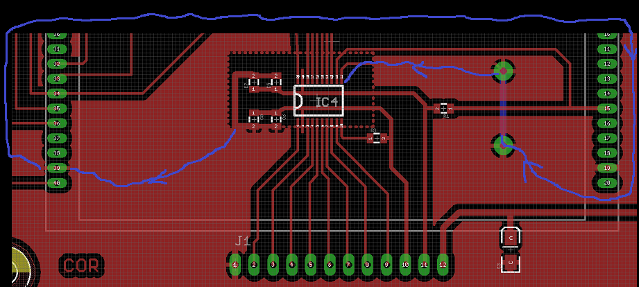
Erm. It's embarrassingly boneheaded actually. I don't have the PCB - I think I jumped on it and I never checked the original design file into source control. I just have a partial backup:

enter image description here

That file is partially routed - eg that keepout box was much smaller at the end and the ground connection at top right IC4 wasn't a tiny line etc etc - but it does illustrate what I did.

IC4 is a TXS0108 level shifter for the 1.8V lines coming up from the bottom. The power lines are decoupled with the caps to its left. When I did the GND flood the grounds were connected and I said "sure, that's fine". No it wasn't. The blue lines illustrate the path from the caps, off to the left, up around the entire top edge of the board (not really shown - it's another 50% in height), down the right and back around to the GND pin on the level shifter.

Horrendous. The darn thing was probably picking up radio! The USB cable on the main board wasn't well shielded (had gold plated connectors though!) and its data transitions coupled across to this loop producing 0.5V spikes on the 1.8V logic transitions. What a mess...

\$\endgroup\$
4
  • 1
    \$\begingroup\$ I really appreciate you sharing.. I learn more from mistakes than successful experiences.. So a ground loop has been formed around the IC? Why did you buy an IC instead of using several MOSFETs? Just curious..... \$\endgroup\$ Commented Jul 16, 2014 at 2:19
  • \$\begingroup\$ And... Are you sure that a ground loop has been created? It seems that the IC has block the loop. \$\endgroup\$ Commented Jul 16, 2014 at 2:35
  • 1
    \$\begingroup\$ I used the TXS0108 because I had two of them remaining from another project. And it's 8 lines. And the chip is cheap(ish). Not sure what you mean by "block the loop". A redesign where the caps were over to the right and the IC pwr/gnd conns were as short as possible made the issues go away. Pin 11 is gnd and there are two Vccs (2 and 19). \$\endgroup\$
    – carveone
    Commented Jul 16, 2014 at 11:15
  • \$\begingroup\$ How did you solve it? Would you like to share the revised part of layout design above? \$\endgroup\$
    – Unknown123
    Commented Nov 25, 2019 at 3:32
2
\$\begingroup\$

The suggestion shown in the first diagram, isn't a very good idea of routing, since it may produce shorts during manufacturing between the track and pad of 0402 package, if strict tolerance is not followed during production.

Since the full routing scenario is shown here, taking the reference from your suggested solutions, it suggest you to follow the second diagram and maintain the track-to-track clearance of 8-10 mils to avoid cross talk between the signal traces.

\$\endgroup\$
2
  • 1
    \$\begingroup\$ Can I ask if 8-10 mils are the rule of thumb number to avoid cross talk? I can hardly agree so, since the distance between pins is around 6 mil... \$\endgroup\$ Commented Jul 14, 2014 at 11:55
  • \$\begingroup\$ Yes, I understand that pitch is not 8 or 10 mils, but since you are not a differential track here in SPI, so easily 8-10 mils of track spacing can be followed. \$\endgroup\$
    – AKR
    Commented Jul 15, 2014 at 4:17

Your Answer

By clicking “Post Your Answer”, you agree to our terms of service and acknowledge you have read our privacy policy.

Not the answer you're looking for? Browse other questions tagged or ask your own question.