3
\$\begingroup\$

I am having an issue with my ADC output.

I am using: 12-bit ADC integrated in a MCU 3.3V voltage reference. Power supply of MCU, ADC and ADC voltage reference sharing the same voltage rail(3.3V)

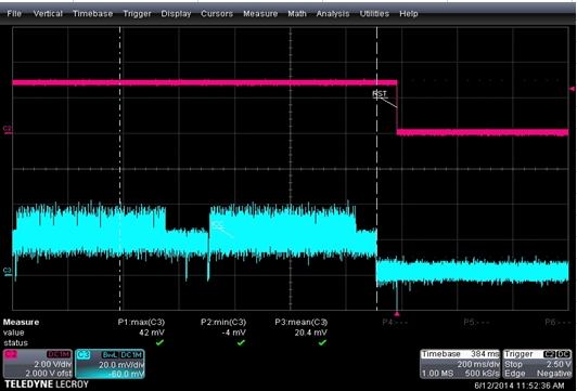
The mean value of my data is ~20mV and I am getting mean value of approximately 20mV, 18mV, 16mV, 14mV, 12mV and 10mV throughout my PCB validation. I will get a random mean value but the mean value will be very close to either one of the values mentioned above.

1st& 2nd attachments are data from development kit.

3rd attachment is oscilloscope measurement for ADC input.

4th& 5th attachment is the data from my PCB which has mean value of 12mV.

6th& 7th attachment is the data from my PCB which has mean value of 16mV.

8th& 9th attachment is the data from my PCB which has mean value of 20mV.

I have 0.1uF tied to ADVREF, ADC power supply.

Is this problem caused by noise within my PCB?

ADC output from development kit

ADC waveform from development kit

Oscilloscope measurement for ADC input signal

ADC output for mean value of 12mV_my PCB

ADC wavform for mean value of 12mV_my PCB

ADC output for mean value of 16mV_my PCB

ADC wavform for mean value of 16mV_my PCB

ADC output for mean value of 20mV_my PCB

ADC wavform for mean value of 20mV_my PCB

FFT 12MHZ ADC spec. FFT_12MHz_ATMEL development lit

\$\endgroup\$

2 Answers 2

2
\$\begingroup\$

Looking at some of those plots you can see discreet jumps in the noise levels which is concerning. You will get some digitization effects in noise levels which shows up in histograms but they discreet jumps in the time domain mean that you are getting some coupling from your board or from the noisy rails.

I think the first step is to get the ADC references off of the same power supply. This could be as simple as adding a series resistor and shunt cap. Ideally you'd have a separate low power regulator.

You haven't given enough information to go much further. A lot will depend upon specifications like PSRR (Power Supply rejection ratio) but reference voltages almost always need to be treated specially.

\$\endgroup\$
11
  • \$\begingroup\$ Yes. I was thinking about the problem of sharing the same 3.3V from a same regulator. I have a series 0 ohm resistor connected between ADVREF and the output of power regulator. I will try to remove it and connect a battery for 3.3V of ADVREF. By the way, what specifications could affect my ADC result? \$\endgroup\$
    – Felix
    Commented Aug 15, 2014 at 10:53
  • \$\begingroup\$ I have changed the ADC reference to a 3.3V battery, however, I still get the similar results mentioned above. I think that there are another 2 possibilities for the problem. First one is 3.3V to my microcontroller(integrated 12 bit ADC I am using) is not clean. Another possibility is the noise from clock signals since one of that is not shielded. \$\endgroup\$
    – Felix
    Commented Aug 18, 2014 at 9:32
  • \$\begingroup\$ YEs, as mentioned, a noisy rail can affect the the results if there is poor PSRR and a jittery clock signal can also affect this, but that will depend upon the internal circuitry. With out further information we'd just be guessing. \$\endgroup\$ Commented Aug 18, 2014 at 11:21
  • \$\begingroup\$ Now only I realized that in the datasheet, VSR is the PSRR you mentioned before. Supply voltage rejection Vout=0.8V SVR is 40dB for the specifications below: VIN = VOUTNOM + 1V +/-VRIPPLE VRIPPLE = 0.1V, Freq. = 1kHz IOUT = 10mA \$\endgroup\$
    – Felix
    Commented Aug 19, 2014 at 2:09
  • \$\begingroup\$ SVR is 30dB for the specifications below: VIN = VOUTNOM + 1V +/-VRIPPLE VRIPPLE = 0.1V, Freq.=10kHz IOUT = 1mA SVR is 15dB for the specifications below: VIN = VOUTNOM + 1V +/-VRIPPLE VRIPPLE = 0.1V, Freq.=100kHz IOUT = 1mA \$\endgroup\$
    – Felix
    Commented Aug 19, 2014 at 2:14
3
\$\begingroup\$

ADCs are not perfect and a 12 bit device with a 3.3V reference will have a theoretical resolution of about 0.8mV. You are seeing variations of a few millivolts and this doesn't surprise me at all - check the INL (integral non-linearity) of the device - it might be +/-3 bits. Check the DC offset spec of the device - this might be anywhere between 2mV and 10mV. Check the DNL (differential non-linearity) of the device - this might be 2 bits.

All these errors add up to make the picture worse.

Also, your 3V3 supply - how accurate is it and how much does it drift? This drift will directly affect accuracy so why not consider using a really tight voltage reference (if it can be applied).

\$\endgroup\$
1
  • \$\begingroup\$ The INL is +/- 1 LSB and DNL is +/- 0.5 LSB. By the way, would you mind to explain a little bit on how the DC offset and the voltage drift may affect the accuracy. Since the ADC input signal is a 3V signal so it would be hard to use a lower voltage as reference. Actually, I tried to add more 0.1uF caps and 1 uF caps on my PCB(cascading on the caps of my PCB) but this doesnt seem to help. \$\endgroup\$
    – Felix
    Commented Aug 15, 2014 at 10:10

Your Answer

By clicking “Post Your Answer”, you agree to our terms of service and acknowledge you have read our privacy policy.

Not the answer you're looking for? Browse other questions tagged or ask your own question.