When working with single-supply op amps biased to mid-supply ( virtual ground rail ) how does one achieve proper bypassing at the IC given that the virtual ground should be as noise-free and stable as possible?
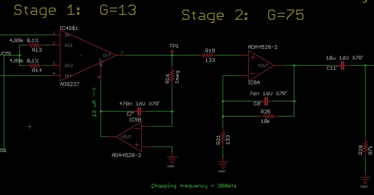
In the schematic below, lets refer to the amp labeled "IC5B":

Power rail is 5V, labeled as +5V/1, and comes from an LDO. The GND of the LD0 is labeled as ISO_GND. VGND is supplied by a 2.5V, +/-10mA reference IC, powered from the same VDD. The ADA4528 is a chopper amp with a chopping frequency of ~200kHz. The amp's VDD pin is connected to +5V/1 and the amp's VSS pin connected to ISO_GND.
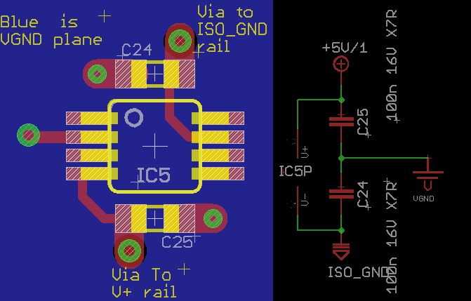
If this were an op amp with dual supplies and didn't care about ground noise, I would bypass each power pin from its respective rail to VGND, like this:

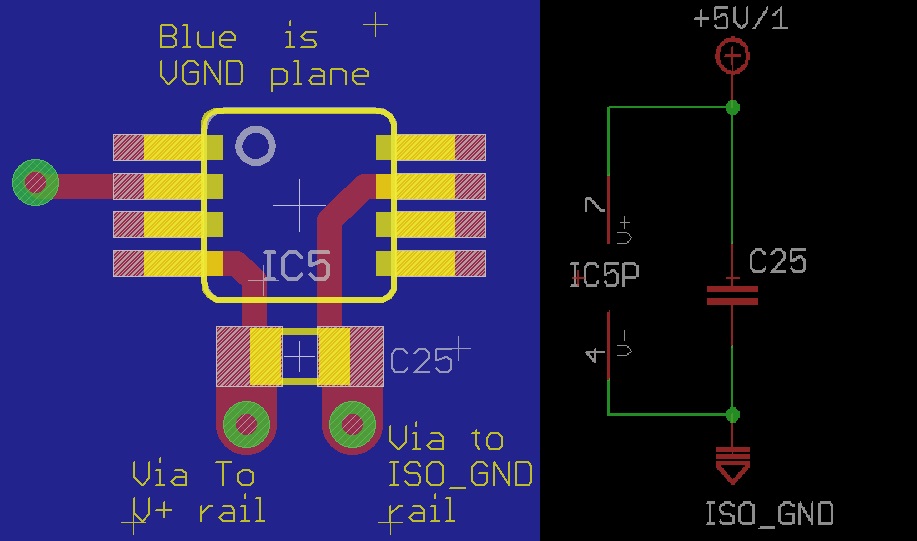
Since the system's entire reference is the VGND plane, and chopper amps draw current in pulses at the chopping frequency, and the op amp's noninverting input pin is connected to VGND and supposed to be noise-free, I am worried about injected noise voltage because of shunted high frequency current into VGND. In that case, would I use only a single bypass cap between the amp's VDD/VSS pins ... like this?

Are there any other considerations from a noise perspective that I should follow in this system?
