1
\$\begingroup\$

I'm trying to interface an ADC chip with my FPGA. The ADC is on a breakout board that fits nicely into my breadboard (.1" pin spacing). The clock input from my FPGA into the breakout board is 12.5 MHz. I also have another clock signal going into a pin that's 3 pins away that is at ~1.5 MHz. I have two questions:

  • Will the 12.5 MHz signal work in a standard breadboard?
  • Will the two clock signals interfere?

All wiring is done from the FPGA Dev board to the breadboard with ~3" jumper wires.

Is there anything else that could go wrong?

\$\endgroup\$
5
  • \$\begingroup\$ "~3" jumper wires" Thanks for playing. \$\endgroup\$ Commented Oct 21, 2014 at 4:32
  • \$\begingroup\$ I don't understand? \$\endgroup\$
    – crocboy
    Commented Oct 21, 2014 at 4:35
  • \$\begingroup\$ The reactance on a jumper that long at 12.5MHz can kill you. \$\endgroup\$ Commented Oct 21, 2014 at 4:36
  • \$\begingroup\$ What do I need to do instead? \$\endgroup\$
    – crocboy
    Commented Oct 21, 2014 at 4:38
  • \$\begingroup\$ Signal wire twisted with a ground wire, wired directly across (no breadboard) stands a reasonable chance of working. \$\endgroup\$
    – pjc50
    Commented Oct 21, 2014 at 10:34

3 Answers 3

6
\$\begingroup\$

12.5 Mhz (80 ns cycle) should be doable.

Wire up your clock lines first. Pick placement that keeps them short and cut the jumpers to length so that you don't have big loopy antennas. Verify that you are getting nice square clocks before wiring the rest.

\$\endgroup\$
3
  • \$\begingroup\$ I agree with Jeff. It's very high for a plug in breadboard but as they are clock signals and not low level signal signals you can probably make it work OK with careful layout, short leads etc - as jeff said. . \$\endgroup\$
    – Russell McMahon
    Commented Oct 21, 2014 at 5:00
  • \$\begingroup\$ I'm getting what looks to be a good square wave (seen with logic analyzer), but every few ms it goes bonkers and gets irregular. Then it goes back to normal. This cycle occurs regularly, I wonder if it has something to do with the signal integrity. \$\endgroup\$
    – crocboy
    Commented Oct 21, 2014 at 15:30
  • \$\begingroup\$ Logic analyzers tend to square-up the waveform. Do you have access to an oscilloscope? Does it do the same thing at the pin with no wires attached? \$\endgroup\$
    – Jeff Bell
    Commented Oct 21, 2014 at 17:31
3
\$\begingroup\$

My suggestions would be (expanding on what Jeff has suggested):

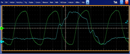
  • Make sure you run a ground from a pin as close as possible to the clock pin to another pin as close as possible to the clock pin. Twist the clock and ground wires together. Keep them as short as possible. Do you have a good high bandwidth scope to check the clock with, so you can see any 'weirdness':

non monotonic edges - from EETimes

  • Add a series terminator of 20-50 ohms (you might have to experiment) at the source of the clock.

  • Give the other clock a ground of its own.

  • Make sure you have plenty of other grounds between the breadboard and the FPGA board.

\$\endgroup\$
2
\$\begingroup\$

Breadboards are crap for high speed. You should look in to making a custom PCB. Install some sort of layout software (kicad, eagle) and then send your design off to OSH park. Probably will cost around $30 and you will have far fewer problems with signal integrity.

\$\endgroup\$

Your Answer

By clicking “Post Your Answer”, you agree to our terms of service and acknowledge you have read our privacy policy.

Not the answer you're looking for? Browse other questions tagged or ask your own question.