0
\$\begingroup\$

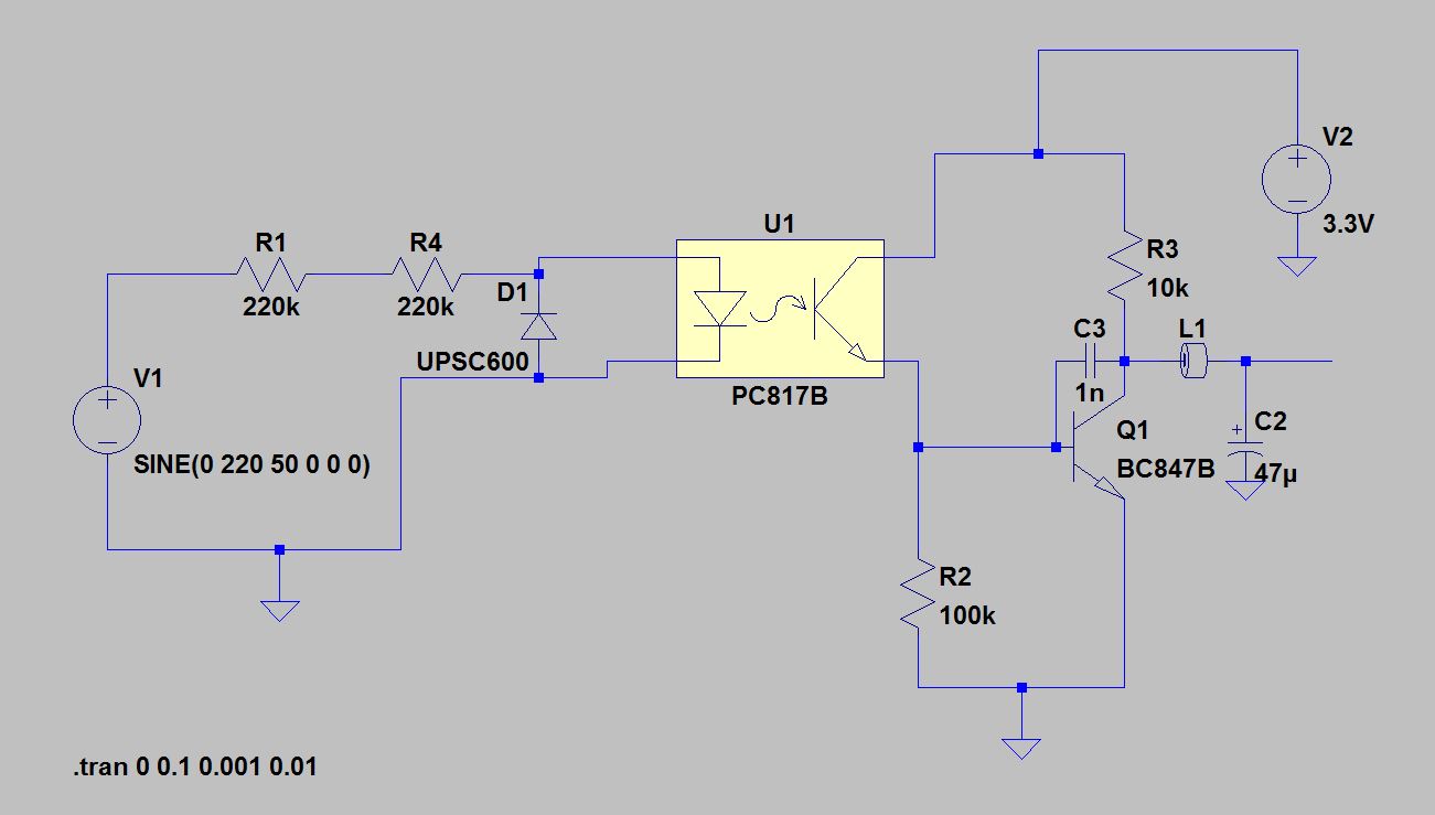
I'm building a circuit that sends TTL level signal to uP whether AC signal exists or not. The schematic is as follows:
enter image description here

Actually, the circuit almost works as I expect; however, there occurs some coupling effect on the emitter side of phototransistor; which cause a delay at the output signal. I also added SPICE simulation of Vout and Vb of BC847B.

enter image description here

Green is Vout, and blue is VbQ1. Vout of the circuit is directly connected to I/O pin of my uP. Two questions arise here:

1) How can I prevent this coupling effect? (I've already tried to couple Vcc to emitter pin of optocoupler.)

2) What is the reason of periodic 90mV increase observed on the output signal? I don't think that it will affect the low-level sensing of uP (Vol = 0.3Vcc); however, it is better to supply a clean zero volt to the uP, I suppose.

Thanks in advance.

\$\endgroup\$
2
  • \$\begingroup\$ Is the negative terminal of the sinusoidal voltage connected to the ground on the low voltage side? If so that may be your problem. Can you isolate these grounds? \$\endgroup\$
    – Alexxx
    Commented Mar 18, 2015 at 12:25
  • \$\begingroup\$ Of course not in reality, but LTSpice doesn't simulate with another GND notation. @Alex \$\endgroup\$
    – ythey
    Commented Mar 18, 2015 at 13:09

3 Answers 3

1
\$\begingroup\$

You're probably fine in regards to the uP's input, but if you're really concerned, you could use a schmitt trigger buffer in between. They're designed for noisy inputs. Or if your particular uP has a built-in comparator as part of its analog stuff, then you could use that also.

As for the ripple, it's because the circuit is only getting pulsed once per AC cycle. Between pulses, it's no different from having lost it entirely. So you have a tradeoff between analog ripple and response time, neither of which can be zero. Such is the problem with sensing AC.

Another approach might be to intentionally pulse the uP at the AC frequency, then have two interrupts:

  1. External interrupt clears a timer and sets the AC_present bit.
  2. Timer overflow interrupt clears the AC_present bit.

If you care about line frequency, you could measure it pretty easily by recording the timer before you clear it and then doing some math with that number.

\$\endgroup\$
5
  • \$\begingroup\$ Considering Vol(max) is about 0.9V, making response time near "0" with trading-off high ripple will not be a problem, I think. But the question is, I couldn't do it yet with simulator. How can I make response time better? \$\endgroup\$
    – ythey
    Commented Mar 18, 2015 at 15:26
  • \$\begingroup\$ R3, L1, and C2 form a lowpass filter. Reduce the time constant/increase the cutoff frequency by reducing any of them. \$\endgroup\$
    – AaronD
    Commented Mar 18, 2015 at 15:35
  • 2
    \$\begingroup\$ By the way, you're going to have a problem when you build this for real. During the ON time, you have 3.3V across U1+Q1 with nothing to limit the current. Depending on your supply, it might collapse briefly and reset whatever else it's powering, or you might blow up U1 and/or Q1. A base resistor for Q1 should solve that problem. \$\endgroup\$
    – AaronD
    Commented Mar 18, 2015 at 15:38
  • \$\begingroup\$ Lowering C2 to 22uF creates an output signal with 0.9ms delay and 160mV ripple. Moreover, I added a 10k base resistor to Q1 as you suggested and Ib become 0.24mA. Theoretically, there shouldn't be a problem for the uP while sensing low level output of this circuit. What do you think for the final configuration? \$\endgroup\$
    – ythey
    Commented Mar 18, 2015 at 15:50
  • 1
    \$\begingroup\$ Sounds good to me. I think you're ready to build it. If your supply is decently substantial, you might want to start with a mid-value resistor between it and your circuit so that you don't blow anything up if you make a mistake somewhere. Too low resistance won't protect it, and too high resistance will prevent it from working. Once it's proven, you can remove/short the resistor if you want and test it again. \$\endgroup\$
    – AaronD
    Commented Mar 18, 2015 at 16:04
1
\$\begingroup\$

Let's take the questions in reverse order:

2) What is the reason of periodic 90mV increase observed on the output signal?

The simplest explanation goes like this: because you are only driving the optocoupler in one direction, the output of the optocoupler/transistor chain is (essentially) a 50 Hz square wave. This is then filtered by R3/C2, but the time constant is only 4.7 msec. Since the on and off periods of 50 Hz is 10 msec each, there is plenty of time for droop to occur on the output during the time when the transistor is off. If you get rid of C2 and look at the output you'll see what I mean.

1) How can I prevent this coupling effect? (I've already tried to couple Vcc to emitter pin of optocoupler.)

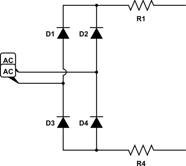
The simplest way is to replace R1/R4/D1 with

schematic

simulate this circuit – Schematic created using CircuitLab

This will provide a much longer drive time with only small dropouts as the AC goes through zero.

The other thing you can do is to recognize that you are grossly underdriving your optocoupler. Your peak LED current is about 0.7 mA (220 x 1.414 / 440 k), while the nominal limit for sustained operation is 20 mA. Admittedly, with more current you get more power dissipated in the resistors, but as it stands you're only producing .06 watts per resistor. At the very least, get rid of one of the resistors.

\$\endgroup\$
2
  • \$\begingroup\$ My idea for using two resistors was not to force voltage ratings of them; however, using high rating one will solve it as you suggested. Though I've already got some good results, I'll apply your suggestions to the design. Is 20mA a strict value for the optocoupler operation? I've driven it with 10mA before without a problem. \$\endgroup\$
    – ythey
    Commented Mar 19, 2015 at 7:32
  • \$\begingroup\$ Look at the data sheet. See operational levels vs. absolute maximum. \$\endgroup\$ Commented Mar 19, 2015 at 12:57
0
\$\begingroup\$

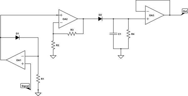
Although what you have presented above uses fewer components and even has the added benefit of mains isolation, another detection circuit that I know of is presented below. Perhaps with added mains isolation between the second stage amp and the peak detector then this circuit could be of use.

schematic

simulate this circuit – Schematic created using CircuitLab

This circuit is generally used as a small signal detector by using an ideal diode op-amp configuration, amplification stage, and a peak detector fed into a buffer. You could possibly make the second stage an attenuator instead.


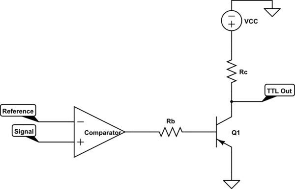
Or something as simple as a comparator, assuming you have appropriately conditioned the mains signal (AC-DC conversion, for example), and a PNP transistor to convert the positive and negative rail voltages that you would get at the output of an op-amp comparator:

schematic

simulate this circuit

In this case, when the conditioned signal is greater than the reference the Op-Amp will rail high and turn the PNP off. In the off state, the TTL_OUT node will be pulled-high through Rc. Likewise, when the signal is less than the reference the Op-Amp will rail low and turn the PNP on. You must design Rb and Rc such that in this situation the transistor will saturate and thereby drive the TTL_OUT node to saturation (~200mV).

\$\endgroup\$

Your Answer

By clicking “Post Your Answer”, you agree to our terms of service and acknowledge you have read our privacy policy.

Not the answer you're looking for? Browse other questions tagged or ask your own question.