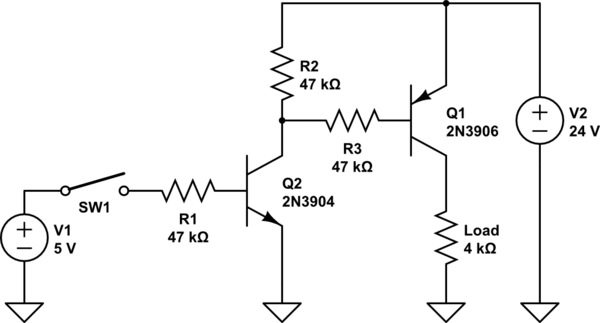
Your circuit should work fine, although I have a couple of minor objections to it.
However, the main reason for this answer is that you got outright bad advice in a comment. No, you don't want to connect the emitter of Q2 to the output. That would make the whole pair a emitter follower, which would only allow the load voltage to go to about 4.3 V, not the 24 V supply. There is no place in engineering for knee-jerk answers and blind application of "rules" without actually understanding the reasons.
Also, here is a simpler answer that accomplishes the same thing:

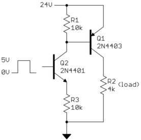
The main difference is that Q2 is now a voltage-controlled current sink. The digital signal can directly drive the base of Q2, and the output of the current sink (the collector of Q2) can be tied directly to the base of Q1.
The load will draw 6 mA. Let's say Q1 can be counted on to have a gain of at least 50. That means its base current must be at least 120 µA. R1 will also take some current. Let's say worst case the drop on R1 is 750 mV, so the extra current needed for R1 is 75 µA, for a total of 270 µA needed to turn on Q1. When the base of Q2 is driven to 5 V, there will be about 4.3 V across R3. Most of the current thru R3 will come from the collector. We need this to be at least 270 µA, so R3 must be no more than (4.3 V)/(270 µA) = 16 kΩ. The value of 10 kΩ shown above leaves some margin.
Working forward, we have about 430 µA thru R3. 75 µA of that comes from R1, with the remaining 350 µA or so from the base of Q1. This means we require Q1 to have a minimum gain of (6 mA)/(350 µA) = 17, which is well within the capability of many small signal PNP transistors.


