0
\$\begingroup\$

I'm still pretty much a electronics-beginner, I'm currently working on modifying a USB game-pad to use switches instead of buttons and I want LEDs to accompany the switches. The basic solution I was hoping to use looked like the following:

schematic

simulate this circuit – Schematic created using CircuitLab

Note that when Input 5V to GND is shorted then IC transmits the button as pressed. The current through the LED is 20mA.

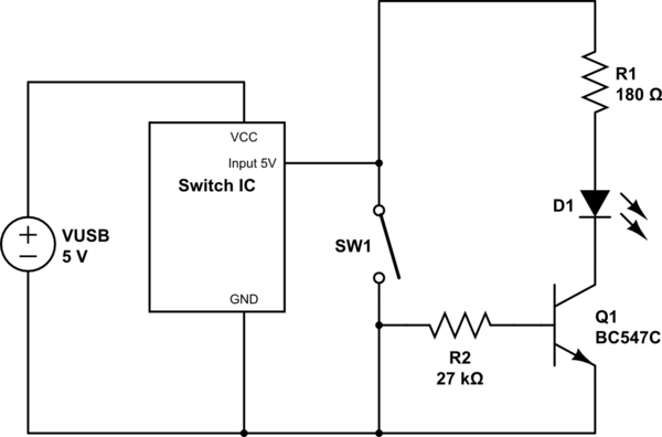
The schematic above makes the LED work but the controller no longer recognizes it as being switched on. So, unable to modify the current going through the switch I instead tried to add a transistor with the resistor and LED separate from the switch, similar to the solution here:
schematic

simulate this circuit

This makes the switch work again but the LED does not power on. It does work when I remove the connection between the switch and GND so I'm assuming all the current goes through the GND-connection and nothing goes to the transistor base. Am I thinking incorrectly or how should I solve this?

\$\endgroup\$

2 Answers 2

1
\$\begingroup\$

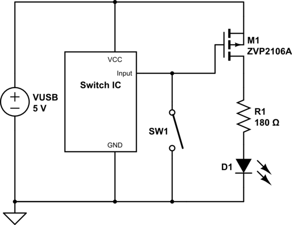
Your original schematic is somewhat confusing, as it does make it look like you are trying to short-circuit the USB power rail. I have redrawn it below with a circuit that should do what you want. It uses the switch to pull down the gate of a P-channel enhancement mode MOSFET.

schematic

simulate this circuit – Schematic created using CircuitLab

The main point to note is that the current to drive the LED no longer comes from the switch IC, but instead directly from the USB power rail. The switch input is not intended to provide significant power, and to get the current amplification benefit from the transistor it needs to get its current from a higher amperage source.

You could achieve this using a PNP BJT, but that will have a fixed saturation voltage across the collector and emitter of the PNP transistor (around 0.15V) requiring a recalculation of R1. It also requires a series base resistor whose value must be calculated with the Hfe of the BJT in mind. It does have the advantage of not placing a low gate threshold voltage requirement on the transistor, and more suitable PNP BJTs are available in through-hole packages than P-channel MOSFETs.

schematic

simulate this circuit

This circuit uses the BC557 purely because it is the complementary part to the BC547 you used in your original attempt. The guaranteed Hfe of the lowest grade (A) parts is 110, so for -20mA collector-emitter current we need at least 180uA of base current. Using a 4k7 base resistor we have 5-0.7 = 4.3V across it, giving a base current of 4.3/4.7k = 915uA. This is enough to drive the BJT hard into saturation without excessive base current flowing. Note that with the MOSFET version of this circuit there would be practically no gate current flowing, so you would gain greater efficiency that way. I haven't changed R1 to allow for the collector emitter saturation voltage - the required reduction would likely be around 10 ohms, so you may choose to neglect this.

\$\endgroup\$
3
  • \$\begingroup\$ I agree, I wasn't making it fully clear that I was shorting an IC input and not the USB rail. I've updated my schematics similar to yours, which is explains it much better, thanks for the great example! Your solution looks good though, I just need to take some time and go over it and study up a bit. One thought on point nr 1 of PNP downsides, if I add a resistor in line with SW1 wouldn't that just put me in the same situation as I'm in now where the IC wouldn't be satisfied? What is the difference between that and putting a resistor in series when using a NPN BJT? \$\endgroup\$
    – SvDvorak
    Commented Aug 29, 2015 at 23:39
  • \$\begingroup\$ I'm going to draw out the PNP solution too - I realised there's actually a less sensitive way of constructing this that will give you two choices to pick from. \$\endgroup\$
    – stefandz
    Commented Aug 30, 2015 at 8:26
  • \$\begingroup\$ I just finishing reading up a bit and I get it now. Sure, it won't be efficient but this is a small hobby-project and those MOSFETs are quite a lot more expensive, I need to do this for a total of 8 switches. I'll order the components and test it out before I'll mark this as the answer. \$\endgroup\$
    – SvDvorak
    Commented Aug 30, 2015 at 18:57
0
\$\begingroup\$

First off your switch in the second diagram will short out the 5V supply when pressed.

Secondly put a resistor in series with the switch and move the lower connection of the switch to connect between R2 and the base of the transistor.

\$\endgroup\$
1
  • \$\begingroup\$ As I mentioned, it's actually not a 5V supply but an IC supplying 5V and I need to short it for the IC to recognize the switch as pressed. So from my testing I can't add a resistor in series with the switch. Would it be more clear if I switched out that component to another in the schematic? I couldn't find a fitting one. If the switch is connected between R2 and the base, would the other end of R2 be connected to +5V? That would nullify the switch wouldn't it? \$\endgroup\$
    – SvDvorak
    Commented Aug 29, 2015 at 13:23

Your Answer

By clicking “Post Your Answer”, you agree to our terms of service and acknowledge you have read our privacy policy.

Not the answer you're looking for? Browse other questions tagged or ask your own question.