4
\$\begingroup\$

Here I asked a question why to have the capacitors:

FT232R chip and capacitor

But now the problem of their proper setup arises i.e. how to include the excerpt at the bottom of the picture in the whole circuit? Also I have a fundamental question here. Isn't it so that when I connect capacitors in a parallel way I could simply use 1 equivalent capacitor with Ceq = C1 + C2 + C3? Thus in my case I would have only 1 capacitor with C = 10nF + 100nF + 4.7uF =~ 4.8 uF. Also why are 10nF and 4.7uF capacitors polarized and 100nF is not? I read that it's more of a technological requirement that larger capacitors ~1uF+ have to be polarized. Why then 10nF is polarized? Thanks.
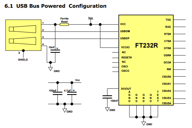
FT232 usb powered

The picture is from http://www.ftdichip.com/Support/Documents/DataSheets/ICs/DS_FT232R.pdf

\$\endgroup\$
1
  • 1
    \$\begingroup\$ I'm intrigued about the polarized 10nF capacitor. I would have to go out of my way to find one since most materials in that range are non polarized. Maybe it's a typo. \$\endgroup\$
    – W5VO
    Commented Oct 4, 2015 at 14:48

3 Answers 3

1
\$\begingroup\$

The various size, style and values of capacitors shown are selected because of the advantages of each type.

Normally the smaller non-polarized capacitor will have better performance at high frequencies.

The larger valued capacitors that are polarized will have ability to work at lower frequency and smooth larger current flows at those frequencies.

Note also that one capacitor is isolated from the others via a ferrite bead so there is not a direct combination possible anyway.

So as you can see there is a disadvantage to combine all the values to a single capacitor.

\$\endgroup\$
3
  • \$\begingroup\$ Michael Karas, why will they be isolated via ferrite bead? It seems that if I am to install the decoupling capacitor as closest to the source as possible, then I would have 100nF, 4.7uF and then immediately 10nF. \$\endgroup\$
    – user51704
    Commented Oct 4, 2015 at 15:59
  • 1
    \$\begingroup\$ The 10nF capacitor and the ferrite bead are supposed to be close to the USB connector and work together as a filter to block RF noise. The 100nF and 4.7uF caps are meant to be placed as close to the FT232R chip's VCC / GND pins as possible. \$\endgroup\$ Commented Oct 4, 2015 at 16:10
  • 1
    \$\begingroup\$ @futer8: the ferrite bead is an inductor (roughly speaking, there's more to it); so that's more or less a pi filter. It's not as if there's just a wire/trace between those (and even just that has substantial inductance at high frequencies). So my rule of thumb is to never combine the small value ceramic caps (which are intended to short very high frequencies locally near each chip). \$\endgroup\$ Commented Oct 4, 2015 at 17:11
1
\$\begingroup\$

There are several questions here which begin to answer your question e.g.Placement of decoupling capacitors

Fundamentally, capacitors are not perfect. Each value will operate most effectively to filter some frequency band of noise, and mitigate the inductance of the power supply and tracks.

Essentially they are trying to provide power to a chip which needs energy very quickly from a power supply which can't respond quickly enough, connected over wires which resist (through inductance) changing the power they supply.

Because the capacitors are supplying power very locally, rather than going across wires (aka PCB copper tracks) they reduce the amount of electrical noise emitted by the 'wires'. The effect of this is Radios, e.g. mobile phone work near the electronics.

The capacitors, especially 100nF, should be mounted as close to the chip as practical. Also, assuming you are making a PCB, try to keep power supply tracks and ground as 'wide' and short as practical to reduce resistance and inductance.

\$\endgroup\$
1
\$\begingroup\$

I could simply use 1 equivalent capacitor with Ceq = C1 + C2 + C3?

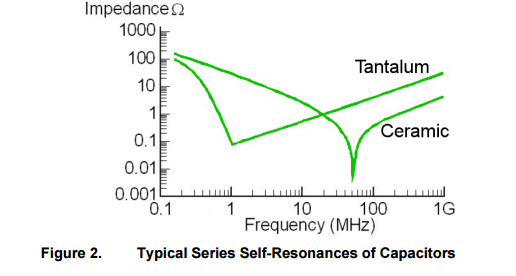
No, you cannot do that here. The various caps have different resonant/corner frequencies. It's okay to add them up when doing say a bulk filter for a power supply (e.g. use two 2200uF in parallel) or the bulk reservoir caps for a board (say several 220uF spread on the board, typically on a diagonal pattern). But you cannot "add up" 100nF + 4.7uF on a supply rail. These two serve different purpose. The larger one (uF) becomes an inductor at high frequency due to parasitics. That's why you need the smaller (nF) one in different tech. Analog's app note MT-101 discusses this in detail. It's about opamps, but applies to the supply rails of most chips. TI has a similar appnote SLOA069; here's an illustrative graph from it (but this is just the general idea regarding the effects of parasitics):

enter image description here

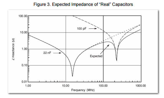
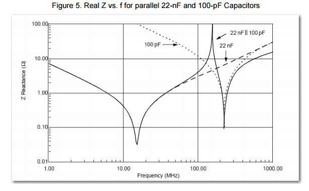
Cypress has a note AN1032 for higher speeds used in data communication. Even if you use the same tech for the caps here's what happens in calculation vs. reality when you parallel them:

enter image description here enter image description here

That's why it's a good idea to go (at least as a start/prototype) with the values recommended in the datasheet for a particular chip. Hopefully the manufactuerer of the IC tested the effect of the combo they recommend on the real chip before putting in the datasheet.

Now, as a matter of practicality, I have combined/added the values of eletrolytics for nearby components, for example I used one 22uF eletrolytic instead of two 10uF ones for nearby opamps (which saves a bit of board space). But I left the ceramics separate for each opamp. I'm not an experienced designer and didn't do sophisticated calculations... and got away with that. I don't know how more sophisticated engineers solve this kind of problem, i.e. combining networks of caps. It's probably hard given all the variables including parasitics.

\$\endgroup\$
2

Your Answer

By clicking “Post Your Answer”, you agree to our terms of service and acknowledge you have read our privacy policy.