11
\$\begingroup\$

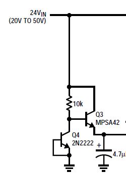
I was reading through Linear Technology's AN70 application note and on Figure 40 there is a part of the circuitry that I can't understand.

It looks like a BJT pass transistor voltage regulator but instead of a Zener diode as a reference it uses a BJT with its base and emitter shorted.

My only idea that it somehow uses the CB diode in reverse conduction as a voltage reference.

Can anyone explain how exactly it works?

Circuit - Figure 40

\$\endgroup\$
0

2 Answers 2

5
\$\begingroup\$

The 2N2222 is maximum rated at 30V for V\$_{CEO}\$ and, considering the circuit says the line voltage can be between 20V and 50V then maybe this circuit is a design to test the breakdown voltage of the 2N2222.

However, figure 40 in AN70 does show it being used as a zener to prevent over-voltage being applied to Vin on the LT1533 - there is no strong evidence that this is a properly tested idea. Sure the 10k resistor limits current into the 2N2222 but it's not a design technique I'd recommend. Just use a 24V zener I would suggest.

You can't rely on the 2N2222 not zenering at 50V and maybe this might exceed the LT1533's Vin value. I'll check....

The LT1533 has a recommended Vin limit of 24V and a maximum rating of 30V so I'd say this was a bad design without strong evidence to the contrary.

\$\endgroup\$
4
  • \$\begingroup\$ According to cr4.globalspec.com/thread/72501 the knee is even sharper than for a Zener. Possibly they wanted to use this effect? \$\endgroup\$ Commented Oct 5, 2015 at 12:04
  • 1
    \$\begingroup\$ @RespawnedFluff - that link is about reverse breakdown of base - emitter junction and not collector-emitter breakdown. \$\endgroup\$
    – Andy aka
    Commented Oct 5, 2015 at 12:07
  • 2
    \$\begingroup\$ I wouldn't put it past Jim Williams to know something about where low-current breakdown starts in a specific transistor that makes this a pretty safe circuit for everyday use. However I'm with Andy : I wouldn't rely on it anywhere critical, and if I used it elsewhere I'd 100% test it in production, and look at the prototypes pretty closely across temperatures... \$\endgroup\$
    – user16324
    Commented Oct 5, 2015 at 12:40
  • \$\begingroup\$ One thing I did find is that the BVCER (collector to emitter voltage breakdown voltage with resistor between base and emitter) is maximized when this resistor is minimized. So that's why the base is shorted to the emitter. The base-emitter resistance is not zero though. \$\endgroup\$ Commented Oct 5, 2015 at 12:49
3
\$\begingroup\$

Compare Figure 40 with Figure 39, and you'll see that the same function in 39 is performed by a zener. I suspect that your transistor in 40 is an error. The emitter should be pointing up, with the base and collector tied together to ground. In this configuration the transistor will function as a ~6 volt zener, and Jim Williams used the circuit freely.

\$\endgroup\$

Your Answer

By clicking “Post Your Answer”, you agree to our terms of service and acknowledge you have read our privacy policy.

Not the answer you're looking for? Browse other questions tagged or ask your own question.