3
\$\begingroup\$

I am studying the Sparkfun Logic Level converter and the basic aim of this is to understand how these BSS138 transistors are used in logic level conversion. I have used transistors before in driving high current motors with MCU's i.e. small time h-bridge configurations. Now I want to use them to make my own logic level converters.

So went to the SparkFun GitHub repo and downloaded the eagle files. Something just does not add up in the schematics for me and I seek clarification around this.

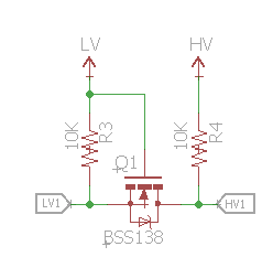
Lets look at how the BSS138 is wired up:

enter image description here

The first thing that strikes me as odd is that I cannot see a earth/ground connection here seems like the low voltage side is connected to the Gate and Source while the High voltage side is connected to the Source.

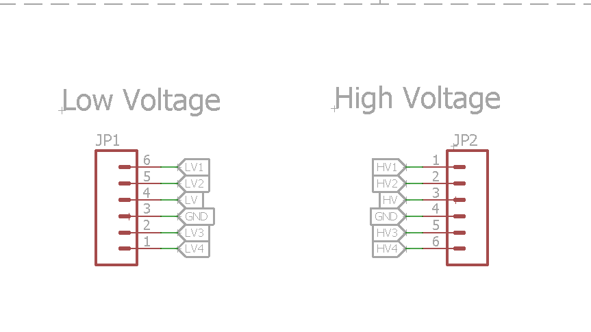
However there is a clearly defined GND on both the HV and LV side of the board designs and on the schematic? See below:

enter image description here

I must be missing something fundamental here.I can even see how current wuld flow without the BSS138 having some sort of grounding.

\$\endgroup\$

2 Answers 2

3
\$\begingroup\$

You are right, in that a common ground is needed between the circuits connected to each port of the translator.

However, this particular circuit fragment depicted in your diagram of the translator out of context does not involve any connections of its own to ground apart from the possible ones through whatever is connected to its ports.

Effectively, this circuit is a sort of bidirectional pass gate, sitting between two pullup resistors which can generate high states. Generating low states is left to the drivers connected to it, which would presumably have some kind of low-side switch that can connect to their shared ground. If either side does that, the other will see the "low" pass through the FET, while if neither does so each sides see a pullup towards its own positive rail.

It would be useful if that schematic diagram had a nice clear net line between the ground ports on each side. It may have been prepared in a style where the name of the ground terminals being common means that they are in fact connected in the netlist (as they would need to be on the PCB), despite this not being shown visually.

Here's an excerpt from the xml-format Eagle schematic:

<net name="GND" class="0">
<segment>
<wire x1="25.4" y1="88.9" x2="27.94" y2="88.9" width="0.1524" layer="91" style="longdash"/>
<pinref part="JP1" gate="G$1" pin="3"/>
<label x="27.94" y="88.9" size="1.27" layer="95" xref="yes"/>
</segment>
<segment>
<wire x1="66.04" y1="88.9" x2="63.5" y2="88.9" width="0.1524"     layer="91" style="longdash"/>
<pinref part="JP2" gate="G$1" pin="4"/>
<label x="63.5" y="88.9" size="1.27" layer="95" rot="R180" xref="yes"/>
</segment>
</net>

Which indicates there there is a named "GND" net having two visually separate segments, which are nonetheless the same net as they have the same name.

\$\endgroup\$
5
  • \$\begingroup\$ I did some digging and the Eagle PCB file/board file does have the ground net on it. I am busy tracing it now. It seems that the schematic is not a complete and slightly misleading. \$\endgroup\$
    – Namphibian
    Commented Dec 4, 2015 at 3:20
  • 1
    \$\begingroup\$ I believe it is complete, it just relies on the convention that nets having the same name are the same net, even when not visually connected. \$\endgroup\$ Commented Dec 4, 2015 at 3:21
  • \$\begingroup\$ I missed this answer on the site. Makes sense now. electronics.stackexchange.com/questions/97889/… Thanks! \$\endgroup\$
    – Namphibian
    Commented Dec 4, 2015 at 3:23
  • \$\begingroup\$ So if I used this in a circuit which is a 5v circuit with a AM1117(or similar) voltage regulator which then outputs 3.3v ,since the 5V and 3.3V have a common ground, theoretically I could ignore the ground connector in this example completely? \$\endgroup\$
    – Namphibian
    Commented Dec 4, 2015 at 3:30
  • 1
    \$\begingroup\$ @Namphibian as long as you have a common ground somewhere in the circuit, then yes you can ignore it. \$\endgroup\$ Commented Dec 4, 2015 at 3:34
2
\$\begingroup\$

The translator itself is indeed not connected to ground, nevertheless the two circuits it is connected to need to be referenced to the same ground for proper operation. We see that the ground pins on your two connectors are connected to the same named net while all the other pins on the connectors are connected to differently named nets.

The way this translator works is as follows.

  • If the "low voltage" side is pulled low then the transistor turns on, joining the two sides together and pulling the high voltage side low.
  • If the "high voltage" side is pulled low then the body diode of the transistor starts to conduct, this pulls the "low voltage" side down turning on the transistor which pulls it down further.
  • If neither side is pulled low then the transistor and it's body diode turn off and both sides are pulled high by their respective pull-up resistors.

Note that the characteristics of the transisitor are quite important. What the circuit sees as a "low" depends on the "low voltage" power rail and the characteristics of the transistor. If the transitors threshold voltage is too high then it may not correctly detect and transmit a low level. If the transitors threshold voltage is too low then it may falsely detect a low.

Also note that this circuit relies on pull-ups to provide the "high", so it is only suitable for relatively slow signals.

\$\endgroup\$

Your Answer

By clicking “Post Your Answer”, you agree to our terms of service and acknowledge you have read our privacy policy.

Not the answer you're looking for? Browse other questions tagged or ask your own question.