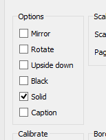
I would like to print Pads, Vias, SMD footprints altogether so that I can apply UV solder mask on board. The problem is that the SMD footprints is part of TOP layer.
What to do?
Looks like correct layer would be tStop, but it appears stripped instead of filled. Looks like I should use some image editing software to fill those pads manually.. .

