Holes move opposite to electrons but up to which point inside the diode?
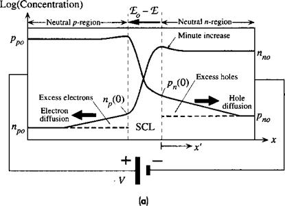
Holes pour across the junction, and flood into the n-type material, forming a moving cloud of opposite carriers which is much wider than the depletion zone.
Don't forget that doping density in semiconductor is typically very small. Most of the silicon is neutral and insulating. Only one in ~million lattice locations supports a free electron, or supports a mobile hole. The mobile carriers behave as a very sparse, easily compressed gas, millions of times less dense than the electron-sea of a metal. When such sparse "opposite gases" come together, the particles don't instantly collide.
So, when the cloud of holes floods into the n-type side, there's plenty of empty space in the lattice, with only very few free electrons there. Occasionally a hole does meet a mobile electron. They fall together, producing neutral (insulating) silicon. The electron cancels the positive hole, and the hole "freezes" the electron in a valence bond so it no longer moves.
In a forward-biased diode, holes are pouring into the n-side, and electrons are pouring into the p-side. As they travel, the electrons in the p-side are being "eaten" by the holes there, and the cloud of electrons gradually disappears, ending up with an exponential-shaped density profile. And, in the n-side, the moving holes are being eaten by electrons, and the cloud of holes gradually thins out to nothing, with similar profile, but not necessarily the same general width. Yes, in the depletion zone some of this "cancellation of opposite clouds" occurs. But many carriers make it past the zone, and flow far into the silicon on the other side before finally
meeting an opposite carrier.
http://elektroarsenal.net/forward-bias-diffusion-current.html

Above is a classic combination-graph of forward-biased diode, showing a graph of hole and electron population density, p-side to the left, n-side to the right. Note that it's a log scale. Note that the depletion layer is thin, while the invading clouds of mobile carriers spread to much wider distance. (In a transistor, they'd spread all the way across the entire base layer!)
PS, some semiconductors have "direct recombination," where holes and electrons 'vanish' upon collision. Silicon isn't this type. In "indirect recombination" of silicon the wandering holes and electrons can only vanish if both have been captured by a lattice defect, dopant ion, etc.
PPS holes definitely do move. (Go and play with an abacus, sliding the beads around, and you'll see the moving holes.) I think many people get confused about this. It's true that protons don't jump between atoms. Only electrons do the jumping. But the jumping of electrons is causing the holes to move through the lattice. Flows of holes, hole currents, these are perfectly real. The real issue is that these aren't proton currents. A "hole" is an exposed proton, an excess positive charge. Whenever an electron then moves in from a neighboring neutral lattice site, it cancels that excess proton, but it also exposes a new excess proton behind. The "excess positive" has moved, the lattice-vacancy has move. Some people insist that holes cannot move, but they are simply wrong. Instead they should insist that positive protons cannot move! A jumping valence-band electron means that the hole has moved through the crystal, but without any protons needing to move.

