221
\$\begingroup\$

What is a decoupling capacitor (or smoothing capacitor as referred to in the link below)?

How do I know if I need one and if so, what size and where it needs to go?

This question mentions many chips needing one between VCC and GND; how do I know if a specific chip is one?

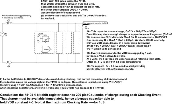
Would an SN74195N 4-bit parallel access shift register used with an Arduino need one? (To use my current project as an example) Why or why not?

I feel like I'm starting to understand the basics of resistors and some places they're used, what values should be used in said places, etc, and I'd like to understand capacitors at the basic level as well.

\$\endgroup\$
4
  • 9
    \$\begingroup\$ They are referred to as decoupling caps (not smoothing caps) in the industry. \$\endgroup\$ Commented Apr 19, 2010 at 13:53
  • \$\begingroup\$ @Brian Thanks for the clarification. I modified the title to make it easier for future users to find (but left the reference in the body to make it searchable via smoothing capacitor). \$\endgroup\$
    – Redwood
    Commented Apr 20, 2010 at 5:20
  • \$\begingroup\$ Should this be merged with electronics.stackexchange.com/questions/2262/… ? \$\endgroup\$
    – davidcary
    Commented Nov 13, 2010 at 23:06
  • \$\begingroup\$ I think it works like smoothing capacitor that is after a "full wave bridge rectifier". \$\endgroup\$ Commented Sep 26, 2015 at 6:49

17 Answers 17

147
\$\begingroup\$

I was the one that asked that question. Here is my rudimentary understanding:

You attach capacitors across \$V_{CC}\$/GND to try to keep the voltage more constant. Under a DC circuit, a capacitor acts as an open circuit so there is no problem with shorting there. As your device is powered up (\$V_{CC}\$=5V), the capacitor is charged to capacity and waits until there is a change in the voltage between \$V_{CC}\$ and GND (\$V_{CC}\$=4.5V). At this point, the capacitor will discharge to try to bring the voltage back to the level of charge inside the capacitor (5V). This is called "smoothing" (or at least that is what I call it) because the change in voltage will be less pronounced.

Ultimately, the voltage will not ever return to 5V through a capacitor, rather the capacitor will discharge until the charge inside it is equal to the supply voltage (to an equilibrium). A similar mechanism is responsible for smoothing if \$V_{CC}\$ increases too far beyond its average (\$V_{CC}\$=5.5V perhaps).

As for why you need them, they are very important in high-speed digital and analog circuits. I can't imagine you would need one for an SN74195, but it can't hurt!

\$\endgroup\$
3
  • 2
    \$\begingroup\$ Thanks for this answer. It conveyed a lot of useful information at a basic enough level that I could understand it. \$\endgroup\$
    – Redwood
    Commented Apr 19, 2010 at 1:07
  • 17
    \$\begingroup\$ To elaborate on this, a decoupling cap is used in the context described above but it also in place to provide somewhat instantaneous current demand to the chip it's "decoupling". You might wonder why such a thing is needed if your supply has sufficient current provisions. To answer this question you must consider that traces in PCBs, and any wire in general, has inductance and as such instantaneous current demand (i.e. at each clock pulse of an MCU) cannot be met quick enough given that current can only change at a given rate through an inductor. The cap acts as a current reservoir of sorts. \$\endgroup\$
    – sherrellbc
    Commented Jul 21, 2014 at 14:50
  • \$\begingroup\$ "I can't imagine you would need one for a SN74195" - This implies you've never worked with 7400 logic. Trust me on this, you need decouplers, and one per IC is a VERY good rule. \$\endgroup\$ Commented Jan 19, 2019 at 16:15
178
\$\begingroup\$

Power supplies are slow...they take roughly 10 us to respond (i.e. bandwidth up to 100 kHz). So when your big, bad, multi-MHz microcontroller switches a bunch of outputs from high to low, it will draw from the power supply, causing the voltage to start drooping until it realizes (10 us later!) that it needs to do something to correct the drooping voltage.

To compensate for slow power supplies, we use decoupling capacitors. Decoupling capacitors add fast "charge storage" near the IC. So when your micro switches the outputs, instead of drawing charge from the power supply, it will first draw from the capacitors. This will buy the power supply some time to adjust to the changing demands.

The "speed" of capacitors varies. Basically, smaller capacitors are faster; inductance tends to be the limiting factor, which is why everyone recommends putting the caps as close as possible to VCC/GND with the shortest, widest leads that are practical. So pick the largest capacitance in the smallest package, and they will provide the most charge as fast as possible.

\$\endgroup\$
3
  • 14
    \$\begingroup\$ Good, accurate answer. Ceramic capacitors are better for high-speed decoupling because they are "faster". The bulk (polarized) tantalum capacitors are only for lower frequency because they are "slow" (due to ESR -- think small RC filter inside the capacitor). When people say "smoothing" capacitor I think more of the bulk capacitance on the output of a power supply, not decoupling at the power pins. I haven't used that term since ENG101. \$\endgroup\$ Commented Sep 24, 2012 at 22:26
  • \$\begingroup\$ Wouldn't the IC always be pulling from the capacitor directly? Not to split hairs here but... \$\endgroup\$
    – cbmeeks
    Commented Aug 21, 2014 at 20:48
  • 1
    \$\begingroup\$ @cbmeeks: If at some moment in time, the supply (including everything but the bypass cap) is outputting 1mA and a device is drawing 1.5mA, the device will draw 1mA from the supply and 0.5mA from the bypass cap. If at some slightly later moment in time the supply has increased to output 1.1mA but the load only draws 1.0mA, then the device will draw 1.0 from the supply and the cap will draw 0.1mA from the supply. \$\endgroup\$
    – supercat
    Commented Dec 25, 2017 at 20:16
60
\$\begingroup\$

Normally called a "bypass cap", because the high-frequency noise bypasses the IC and flows directly to ground, or a "decoupling cap", because it prevents the current draw of one IC from coupling into another IC's power supply.

"how do I know if a specific chip is one?"

Just assume they all do. :) If a chip is drawing current intermittently, it will cause the supply voltage to droop intermittently. If another chip is "downstream", it will see that noise on its power pins. If it's bad enough, it can cause errors or noise or whatever. So generally we put bypass caps on everything, "upstream" from the IC. (Yes, the orientation of the traces and the locations of the components matters, since copper is not a perfect conductor.)

\$\endgroup\$
4
  • 7
    \$\begingroup\$ Here is an interesting rule-of-thumb that I found from a document that TI wrote (its in the order of: TYPE then MAX FREQUENCY) Aluminum Electrolytic, 100 kHz; Tantalum Electrolytic, 1 MHz; Mica, 500 MHz; Ceramic, 1 GHz \$\endgroup\$
    – Kellenjb
    Commented Apr 18, 2010 at 13:45
  • \$\begingroup\$ You match my definition of bypass and decoupling cap. Glad to hear one more soul has read just too much. \$\endgroup\$
    – Kortuk
    Commented Apr 21, 2010 at 13:09
  • \$\begingroup\$ Can you add more about upstream and downstream cases? \$\endgroup\$
    – abhiarora
    Commented Jun 10, 2017 at 18:14
  • \$\begingroup\$ @abhiarora Pretend all the wires in your schematic are resistors and think about where the capacitor should be to get the best filtering \$\endgroup\$
    – endolith
    Commented Jun 10, 2017 at 19:52
37
\$\begingroup\$

A smoothing capacitor (a.k.a. decoupling capacitor ) is used to reduce the change in power supply voltage. When you draw high currents from your power supply (like when digital logic switches state) you will see a change in supply voltage. Switching tries to draw large instantaneous currents and produces a voltage drop due to the impedance of the voltage source and the connection between the voltage source and the IC. A decoupling capacitor will help to maintain (or smooth) the supply voltage at the device. Placing this storage element close to the IC reduces the change in voltage at the IC.

Unless you measure the supply voltage at each IC when the IC is drawing its maximum switching currents it is difficult to say how effective the capacitor will be. For most digital devices the recommendation is 0.1uF ceramic very close to the device. Since the capacitors are small and low-cost most designers will just add the capacitors. Sometimes if I have two logic devices that are very close you may be able to orient a single capacitor between two ICs. This is usually not the case.

Power supply ICs have larger smoothing capacitor requirements since the swithing currents are larger. For those devices you need to look closer at the application ripple requirements to determine the appropriate filtering capacitor.

\$\endgroup\$
36
\$\begingroup\$

Just to add more on EM emissions.

Most companies will recommend 0.1uF caps at each power input. Keep in mind this is only the bare minimum required to avoid voltage dips that could effect operation. If you're building a PCB board that needs to pass FCC Part 15 for emissions you need to go further.

Ultimately you need to calculate the entire capacitance needed on the power supply plane based on the PCB design and power usage. A general rule of thumb I use as a starting place is one 10uF tantalum cap per major IC (microcontroller, ADC, DAC, etc) and then a 0.1uF and a 10nF cap at every power pin on every IC. The 10nF caps need to be small—preferably 0402 or at most 0603 sized—to avoid the lead inductance from the package nullifying the effect of the capacitor.

I highly recommend this book if you plan to get into high speed digital design, high speed meaning anything over 1MHz really.

\$\endgroup\$
4
  • \$\begingroup\$ +1 for mentioning the 10nF caps. 0.1uF is good for default, but the 10nF or even 1nF caps will have lower impedances at high frequencies because they have lower parasitic inductances. \$\endgroup\$
    – Jason S
    Commented Apr 22, 2010 at 12:39
  • 7
    \$\begingroup\$ Parasitic inductance is dominated by the package size, not the total capacitance. Sure, there's a correlation between maximum capacitance and package size, so you're mostly right, but a 10nF cap in a 0805 package will have about the same parasitic inductance as a 10uF in an 0805 package. The corollary is that if you have 100 nF cap in an 0603 package, adding a 10nF cap in an 0603 package isn't going to help you very much, if at all. \$\endgroup\$
    – ajs410
    Commented Apr 12, 2013 at 22:12
  • 1
    \$\begingroup\$ And let's not forget that EMI is not always fixable by adding caps. As Hitler discovered youtube.com/watch?v=eeo8ZZTfwZQ \$\endgroup\$ Commented Jan 19, 2019 at 16:18
  • \$\begingroup\$ Did I understand it correctly , 2 capacitor for major pin (10uF,100nF) and 1 for every minor pin (10nF) ? \$\endgroup\$
    – Mordecai
    Commented Oct 31, 2019 at 15:29
23
\$\begingroup\$

Questions related to decoupling seem to be coming up a lot lately. I gave a detailed answer here: Decoupling caps, PCB layout

That talks about decoupling issues and layout. Power supply smoothing is a totally different matter. That generally requires larger caps that have to be able to store a reasonable amount of energy since the power supply ripple frequency is much lower than the frequencies decoupling caps are intended to handle.

\$\endgroup\$
14
\$\begingroup\$

I would like to emphasis one of jluciani's points. It is very important to put the capacitor as close to the chips power input as possible. This can help eliminate any noise that is introduced any where else, either in your circuit, from the power supply, or even some noise being radiated from a source off of your board.

jluciani is correct that 0.1uF is very common for being placed next to ICs. Simply think of the capacitance as how much charge the capacitor can hold, so the bigger the capacitance the more charge it is holding. If you put capacitors in parallel, you add more capacity resulting in a higher effective capacitance.

As far as your question about if that chip needs it or not, I would say, it wouldn't hurt. The datasheet will usually specify if the chip needs decoupling (aka smoothing) capacitors and if so what the recommended value is.

\$\endgroup\$
14
\$\begingroup\$

Just to add a few points to the other answers:

To measure the effects of the current spikes on the supply voltage you'd need a fast oscilloscope. It depends on the speed of the circuits, but I guess you'd need 200MHz to 1GHz bandwidth.

Also, if the power supply circuit carrying the current spikes is large then it will cause radio emissions, which is frowned upon for various technical and legal reasons. A bypass capacitor acts like a shortcut for these spikes, so there is much less emission.

\$\endgroup\$
1
  • 5
    \$\begingroup\$ Most voltage spikes are visible even on a 100MHz oscilloscope since their frequency is related to your clock. An ATmega running at 8MHz will show a spike every 1/8MHz = 125ns. \$\endgroup\$
    – jpc
    Commented Apr 20, 2010 at 9:09
11
\$\begingroup\$

In a general case, some or many ICs, transistors or valves (tubes) will be connected to the same power supply. As a device in these situations operates, it draws varying amounts of current from the power supply in accordance with the signal passing through it. As power supplies are not perfect, the varying current causes a varying voltage to appear on the supply rails. All the other devices connected to the same power supply will then feel this voltage ie. a noise signal will be coupled into them. This may cause instability in analogue circuits or wrong switching in digital ones. By placing DEcoupling capacitors at points described above, the power supply voltage becomes more stable, and the devices are decoupled from each other.

\$\endgroup\$
11
\$\begingroup\$

Bypass caps are sufficiently cheap that in many cases there's no reason not to put them everywhere. If space or cost are extreme issues, however, it may be reasonable to leave off a few. The key is to recognize what may happen if they are left off. My suggestion would be to assume a worst-case scenario if they're left off: (1) RF radiation at the input switching frequency may be increased, and (2) any time an input switches, assume the device's outputs and internal state may be arbitrarily glitched. If either of these behaviors would be a problem, bypass caps are required. If neither would be a problem (e.g. because none of the inputs switch often enough for radiation to be a problem, the device has no internal state, and nothing will care about the state of the outputs at the moments when the inputs are switching) then bypass caps may be omitted.

\$\endgroup\$
9
\$\begingroup\$

Often the datasheet for the chip specifically calls out how many and what size capacitors to use. If it doesn't, best practice is to attach a 1 uF cap to the power pins of each chip, plus a larger cap somewhere on the board. (Before 2001, best practice used 0.1 uF caps).

p.s.: have you considered using a 74HC595 or 74HC166 rather than the 74195? I suspect that would work just as well, and free up some pins on your Arduino.

\$\endgroup\$
5
\$\begingroup\$

People typically give one explanation when asked what the function is of decoupling capacitors, but the truth is they fulfil several tasks.

Here is the list of things I am aware of:

They reduce ground bounce

Ground bounce is a phenomenon where a changing voltage difference across the ground plane negatively affects (mostly) analog and (sometimes) digital signals. For analog signals, like audio for example, this could manifest itself in the form of high pitched noise. For digital signals it could mean missing / delayed / fake signal transitions.

The changing voltage difference is caused by the creation and collapse of magnetic fields caused by changing current flows.

The longer the path the current flow has to follow, the higher the inductance associated with it and the worse the ground bounce becomes. Multiple current flow paths also exacerbate the problem, as well as the speed at which the current changes.

Current flow obviously occurs between a power supply and a connected IC, but somewhat less obviously also between "communicating" ICs. The current flow associated with two ICs looks like this; power supply -> IC 1 -> IC 2 -> Ground -> power supply.

A decoupling capacitor effectively decreases the length a current path by functioning as a power source, thereby decreasing inductance and thus ground bounce.

The previous example becomes; Cap -> IC 1 -> IC 2 -> Ground -> Cap

They keep voltage levels stable

There are two reasons why voltage levels fluctuate:

  • Trace/wire inductance decreases the maximum rate of change of current through that trace/wire; a sudden increase in 'demand' for current will result in a drop in voltage; a sudden decrease in 'demand' for current will result in a spike in voltage.
  • Power supplies (especially those of the switching type) need time to respond and will slightly lag behind current demand.

A decoupling capacitor will smooth current demand and reduce any drops or spikes in voltage.

They CAN reduce EMI (transmission)

When we talk about electromagnetic interference, we are either referring to the transmission of unintended electromagnetic interference or the receiving of intended or unintended electromagnetic signals that are interfering with the function of your device. Typically it refers to the transmission itself.

The placements of (decoupling) capacitors between power and ground planes changes the transmission coefficient across a range of frequencies. Apparently using only one value for your capacitors for the entire PCB as well as lossy / high resistance capacitors is the way to go if you need to reduce EMI, however this goes against common practice (which advocates an increasing order of capacitance the closer you are to the power supply). Most people don't really concern themselves with EMI if they make circuits for their hobby (though radio amateurs typically do), but it becomes unavoidable when you are designing a circuit for mass production.

A (decoupling) capacitor CAN reduce unintended electromagnetic radiation being produced by your circuit.

To answer your remaining questions..

How do I know if I need one and if so, what size and where it needs to go?

Typically you place a decoupling capacitor whenever possible, choosing the smallest physical size with the largest value as close as possible to the power supply pin of the IC.

Would an SN74195N 4-bit parallel access shift register used with an Arduino need one? (To use my current project as an example) Why or why not?

It would probably work fine, but why bother with 'probably' if you can increase the odds by placing a component that costs a few cents, even a single cent in some cases?

\$\endgroup\$
5
\$\begingroup\$

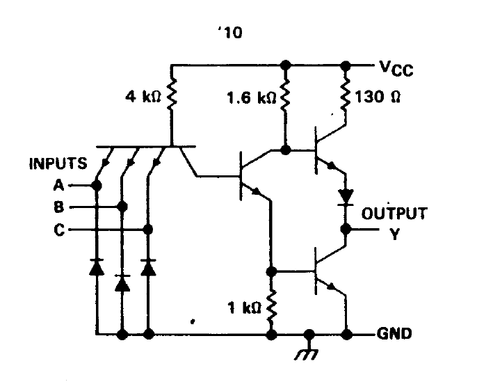
Lets take away some of the magic about bypass caps, by improving the circuit model; 7410(triple NAND) family gates look like this: enter image description here

with shoot-thru current (ignoring currents thru 4Kohm and 1.6Kohm) computed as $$(5v - 3 * Vdiode)/130 Ohm$$ or 5-2.1/130 = 2.9/130 ~ 22 milliAmps.

This gate, available 3-in-one-package, provides high drive (large fanout) and fast speed. Inside a 74195, we don't need all that drive. We do need speed. We'll assume a 2mA shoot-thru per gate (~~15 gates per FF)

schematic

simulate this circuit – Schematic created using CircuitLab

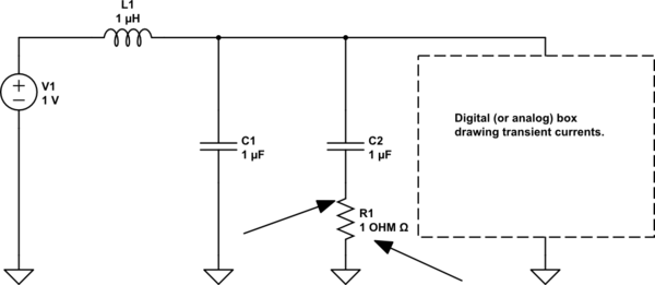
We need to store enough charge for 1uS of busy clocking activity. WHY? Why use 1uS? Because big capacitors and long wires will RING, and upset the VDD at the IC, unless dampened. What ringing frequency? 1uH and 1uF produce 0.159KHz. How to dampen?

Use Q=1 [defined as Q = ZL/R = 2(piFringL/R) ] and Fring = 1/2*pisqrt(LC), we find Rdampen = sqrt(L/C). For 1uH and 1uF, need ONE OHM.

Consider this circuit for good control of VDD ringing:

schematic

simulate this circuit

What does Signal Chain Explorer tell us about this 1_ohm dampening?

enter image description here

Surprise? The logic engineer also needs to DESIGN the VDD filtering and the VDD dampening.

\$\endgroup\$
1
  • \$\begingroup\$ It seems that you accidentally posted the same answer twice and should remove one. \$\endgroup\$
    – Rev
    Commented Mar 15, 2017 at 9:59
3
\$\begingroup\$

Pretty much every IC should have a decoupling capacitor. If nothing is specified by the datasheet, at a minimum, put a 0.1 uF ceramic cap near the power pin of the IC, rated for at least twice the voltage that you are using.

Many things will require more capacitance on the input. You can often find those recommendations in datasheets, app notes, or evaluation kit schematics.

\$\endgroup\$
3
\$\begingroup\$

To answer you question in short: DC does not pass through the capacitor, AC does. Most noise is AC coupled noise, or/and has AC characteristics, i.e. switching +- some DC value. To accommodate these changes, you use a DECOUPLING capacitor. It simply shorts AC signals out. There is an abundant sea of great app notes on why and how they work: http://www.analog.com/media/en/training-seminars/tutorials/MT-101.pdf

Also, the talk about reservoir/smoothing capacitors - bringing it up in this thread just confuses newcomers in terms of terminology.
Smoothing is done to create a very steady voltage. E.g. Some sensors/circuits' outputs are dependent proportionally to their supply voltage. Ripples in the supply will directly affect their output.

\$\endgroup\$
3
  • 1
    \$\begingroup\$ For logic IC's, "decoupling" capacitors are absolutely acting as a reservoir, providing a low impedance path for high switching currents. So I don't think the terms "reservoir/smoothing" are confusing with respect to this question. \$\endgroup\$
    – Rev
    Commented Mar 15, 2017 at 10:06
  • \$\begingroup\$ Capacitors are by definition reservoirs of charge. Smoothing happens for both large and small capacitors. It really ends up being a discussion of semantics, which for the uninitiated may create even more confusion. However, p. 2 from the analog app note sums it up in a nice manner: A large electrolytic capacitor (typically 10 µF – 100 µF) no more than 2 in. away from the chip. The purpose of this capacitor is to be a reservoir of charge to supply the instantaneous charge requirements of the circuits locally so the charge need not come through the inductance of the power trace. \$\endgroup\$
    – Andreas HD
    Commented Mar 15, 2017 at 12:26
  • \$\begingroup\$ A smaller cap (typ. 0.01 µF – 0.1 µF) as physically close to the power pins of the chip as is possible. The purpose of this capacitor is to short the high frequency noise away from the chip. \$\endgroup\$
    – Andreas HD
    Commented Mar 15, 2017 at 12:27
2
\$\begingroup\$

They are needed to lower the power delivery system's impedance. At high frequencies power supplies present a non negligible series impedance mainly due to the inductance of the power nets. Take a look at the "Rail collapse in Power Integrity" section of the following article that can help you understand the idea : https://www.cohenelec.com/considering-capacitor-parasitics/

\$\endgroup\$
1
  • 3
    \$\begingroup\$ It might be good to take some of the information and quote it from the article in the answer as links go down. \$\endgroup\$
    – Voltage Spike
    Commented Jan 16, 2018 at 22:46
1
\$\begingroup\$

Capacitor is storage element and it will save energy in the form of charge. Coming back to decoupling cap, it's also called as bypass capacitor since it will bypass supply ripple and this charged cap will try to maintain fixed dc voltage at VDD pin.

\$\endgroup\$

Your Answer

By clicking “Post Your Answer”, you agree to our terms of service and acknowledge you have read our privacy policy.

Not the answer you're looking for? Browse other questions tagged or ask your own question.