0
\$\begingroup\$

I have a DC SSR (Phoenix Contact 2964270) configured with an input of 0 - 5 VDC. It is trying to trigger a system with a sinking input SSR (Phoenix Contact 2966595). I have a 10K pull down resistor connected to the output of my SSR.

When I disconnect my cable and I connect the device's A2 input to it's 0V it successfully triggers.

When I measure the voltage with my SSR on I see 24VDC. When my SSR is off it only drops down to 14.3 VDC.

Here is a link to my SSR's spec sheet and the device's SSR spec sheet.
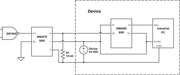
schematic

simulate this circuit – Schematic created using CircuitLab

What do I need to do to get this A output closer to 0V to trigger?

\$\endgroup\$
8
  • \$\begingroup\$ Is your PLC input source or sink? You also need to add references to the schematic so that we know where you're measuring voltages. "When I measure the voltage with my SSR on ...". Where are you measuring? \$\endgroup\$
    – Transistor
    Commented Apr 15, 2016 at 23:44
  • \$\begingroup\$ It is a TTL nand gate from an SN7400. So I believe it is driven both directions. \$\endgroup\$ Commented Apr 15, 2016 at 23:47
  • \$\begingroup\$ You're showing a 24 V circuit connected to the input of your PLC. It can't be a 7400 TTL chip. Is you PLC input source or sink? \$\endgroup\$
    – Transistor
    Commented Apr 15, 2016 at 23:49
  • \$\begingroup\$ There is no PLC. The input to the device is sinking from my A output. The industrial PC that has a sourcing input. I modified the schematic to make that more clear. I as a mentioned in the text I can trigger the device by connecting 0V directly to the device input at A2. \$\endgroup\$ Commented Apr 16, 2016 at 0:01
  • \$\begingroup\$ Can you try without the pulldown resistor? \$\endgroup\$ Commented Apr 16, 2016 at 0:27

1 Answer 1

1
\$\begingroup\$

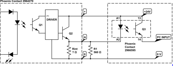
The real problem is that you have chosen the wrong opto-isolator. The 2964270 is a pull-up device. You needed something more like the 2966595 in a 5 V input version so that you could pull A2 on the customer's device down to 0 V. You seem to have realised this and added R1 but set it way too high.

The OPT-24DC/ 24DC/ 2 (used in the customer device) states that to get a logic 1 you need > 16 V across its input. It also states that typical current at 24 V will be 7 mA. (It will probably be only about 4 or 5 mA at 16 V.) To get it to turn on your R1 value needs to pull A2 to less than 8 V. A 560 Ω resistor will pass 14 mA at 8 V so it would suffice. Bear in mind that when your opto turns on that Q2 will connect that resistor to +24 V and the current through it will be 42 mA with power dissipation of > 1 W.

schematic

simulate this circuit – Schematic created using CircuitLab

Figure 1. A more complete schematic.

\$\endgroup\$
6
  • \$\begingroup\$ The current schematic should show that the 2966595 is a four terminal module. The "device" I am referring to comes to us wired as a sinking interface. I'm just showing the relevant section that I'm trying to drive. Changing their wiring is a lesser option than changing things on my side. \$\endgroup\$ Commented Apr 16, 2016 at 10:18
  • \$\begingroup\$ The logic on my side involves a USB Counter board that has 5 VDC I/O. I am converting to 24 VDC to match the customer's device interface. \$\endgroup\$ Commented Apr 16, 2016 at 10:21
  • \$\begingroup\$ Right. That info should have been in the original question. I've edited my answer. See the fourth point in the bulleted list. \$\endgroup\$
    – Transistor
    Commented Apr 16, 2016 at 10:27
  • \$\begingroup\$ Since rewiring the customer's device is not a permanent option, you are saying a pull down resistor is not enough. I need to change out my 2964270 SSR with a different SSR that can do push-pull? \$\endgroup\$ Commented Apr 16, 2016 at 10:44
  • 1
    \$\begingroup\$ Thanks for accepting the answer. A tip for your schematics: logical flow should normally read from left to right (which you did) and potential or voltage from top to bottom so that currents tend to flow from top to bottom. (Your optos were upside down and 24 V rail was low down in the diagram.) Otherwise it's difficult to read. \$\endgroup\$
    – Transistor
    Commented Apr 17, 2016 at 7:31

Your Answer

By clicking “Post Your Answer”, you agree to our terms of service and acknowledge you have read our privacy policy.

Not the answer you're looking for? Browse other questions tagged or ask your own question.