3
\$\begingroup\$

Before entering in to problem:

My application is a laser pulse detection. In this process, when a laser pulse falls on a photo diode, it generates current. Later stages include a I-V conversion, gain, difference amplifier and comparator.

My current problem with I-V conversion can be seen here.

My pulse characteristics:

pulse width min: 10 ns max: 150 ns rise/fall time: 2 ns - 5 ns pulse to pulse width:22 µS

How I selected the opamp for gain and difference amplifier stages

Key parameters: BW - bandwidth and SR - Slew Rate

From this literature I found my BW can be calculated by the formula:

BW = 0.35/(rise time) = 0.35/5 ns = 70 MHz

Now the slew rate is to be calculated:

SR = 2 * 3.14 * BW * Vp = 2 * 3.14 * 175 MHz * 4 V = 2198 V/µs

So matching both these parameters is a CFA AD8003 from Analog. When I go for high slew rates and high BW almost all opamps avaliable are CFA's!

What is worrying me?

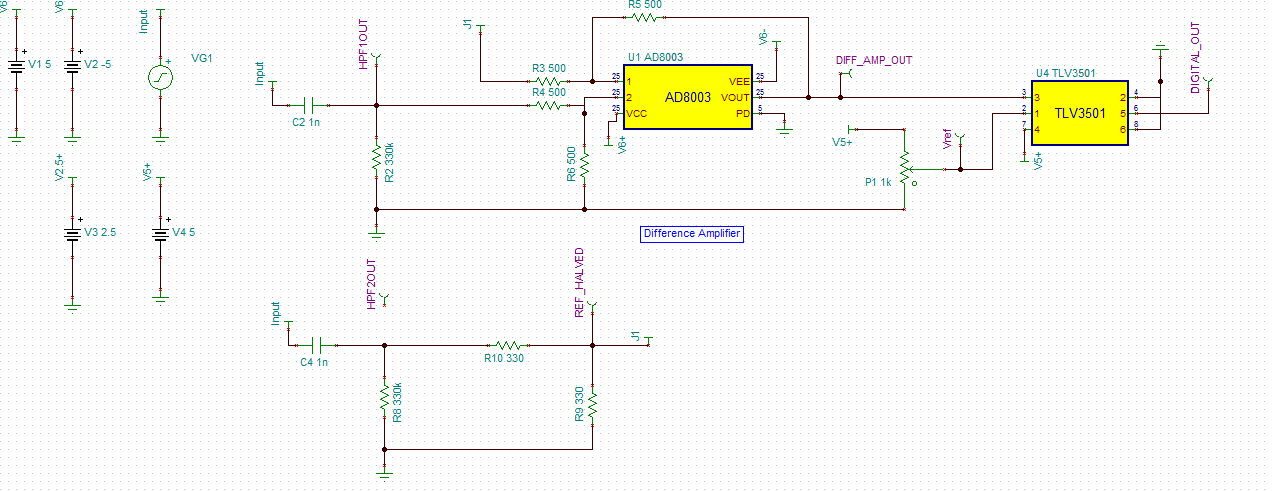
Without any notion when I used CFA for my difference amplifier stage, with unity gain using a 500 ohm resistor for Rf and Rb, the results seemed stable, but it is this statement from Texas Instrument technical literature, clearly saying:

the first difference between voltage feedback and current feedback—the input impedance of current feedback op-amp inputs is very different. Because the inverting input has low impedance, current feedback amplifiers are not good for balanced systems such as differential amplifiers

CFA as difference amplifier

Enter image description here

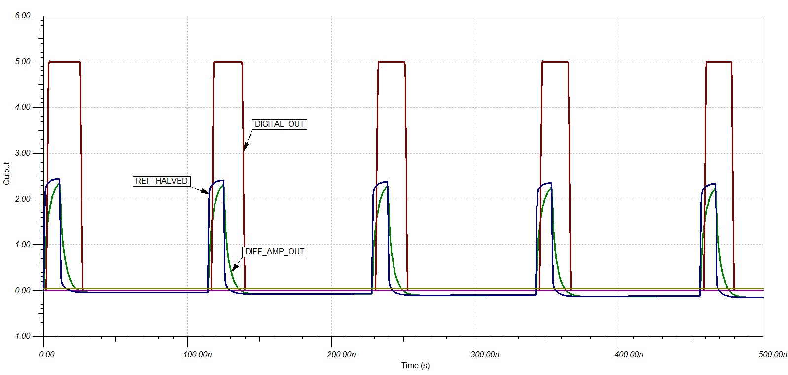
So my results are like this for a difference amplifier followed by a comparator. The pulse here is 10 ns width and 1 ns rise and fall times and repeating at a 150 ns rate.

Enter image description here

Why is the pulse quite expanded? Which capacitor stage has done it I didn't understand.

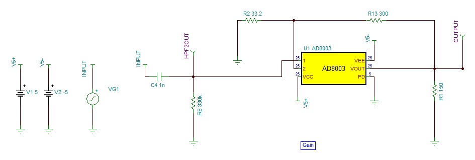
CFA as amplifier with gain

Enter image description here

The results for the above circuit are also not as desired (I just see 0 V output), why so?

\$\endgroup\$
1
  • \$\begingroup\$ CFAs have a low impedance at the inverting terminal (like the base of a transistor), while VFAs has high impedances on both inputs, VFA bandwidth*gain in kinda fixed, so more gain = less bandwidth, whereas a CFA doesn't have that limitation and can give lots of bandwidth even at high gains \$\endgroup\$
    – Sam
    Commented May 2, 2016 at 3:42

3 Answers 3

1
\$\begingroup\$

There is nothing is wrong with your circuit. The wide pulse width is because you're feeding your diff_amp_out to a comparator.

It can only supply you with a pulse of full voltage if the input (in this case) is even slightly above zero volts. I like how your scope shows the tiny delays from stage to stage.

You could adjust the 'trip' level of the comparator, but the output will always be +5 V.

If you just want to amplify diff_amp_out, add another AD8003 op-amp and set your gain to fit your needs. At least you keep your true signal pulse width. Admittedly, working with these nS pulses is tough.

CFA amps are designed for current feed back, which lowers the input impedance, but greatly increases its bandwidth and high frequency response compared to VFA.

All video and RF amplifiers are the CFA type. The VFAs are best for audio and precision DC measurements.

\$\endgroup\$
2
  • \$\begingroup\$ my question why the difference amplifier output is quite different, i mean a charge and discharge kind of , rather than a narrow pulse similar to input \$\endgroup\$
    – kakeh
    Commented May 2, 2016 at 5:20
  • \$\begingroup\$ @kakeh. The slew rate at the outputs depends on the load and/or feedback resistor. Normally these frequencies are piped through 75 ohm impedance circuits (look at some rf stuff online). I would keep lowering those values at the IC output to sharpen the waveform rise and fall times until the amps drive limit is reached. Possibly 150 ohm for load and 150 ohm for feedback. \$\endgroup\$
    – user105652
    Commented May 2, 2016 at 18:42
1
\$\begingroup\$

You have to start from the photodiode + input transimpedance amplifier design. To get that speed easily you likely should limit yourself to a small (1 mm2 or so) low capacitance photodiode.

Then you should get into tricky high-speed transimpedance photodiode amplifier design (you can google a lot), e.g.:

It is all about noise/BW/DC limit optimization. If your signal is strong enough, so you don't care about noise - it is easier. In the simplest case of a very strong signal you can use just shunt resistor. If you don't care about the DC component you can use an RF pulse transformer (balun) to convert impedance 1:4, get signal into 50 ohm coax (12.5 impedance visible to the photodiode) and use the Minicircuits ZFL-1000 amplifier or similar.

For best signal/noise at high speed one can use an avalanche photodiode, PMT (depending on the wavelength) or even SiPm (Sensl, etc.).

\$\endgroup\$
1
  • \$\begingroup\$ what you said about photo diode capacitance is absolutely right, that is the main culprit in entire pulse shaping, but for now i have to go with the PD having 12pF capacitance, since few days i was been working on what you shared, you can answer my noise analysis problem : electronics.stackexchange.com/questions/237600/… \$\endgroup\$
    – kakeh
    Commented Jun 3, 2016 at 15:34
0
\$\begingroup\$

I have some doubts about your design.

First, it seems, the whole amplifier AD8003 has no meaning: you first attenuate input signal 2 times by R4 R6 then you amplify it 2 times by U1 R3 R5. Why not to send the input straight to high speed comparator?

The rise / fall times of your optical signal are so short that you can not improve signal quality by AD8003, you only make it worse, as we see from your pictures.

Second, R2 in parallel with R4 R6 has no meaning.

So - the basic question is: what for do you use AD8003 stage?

\$\endgroup\$
1
  • \$\begingroup\$ its a generic circuit, the R2-C2 and R8-C4 are HPF of fc=5Mhz, the R4 - R6 and R3- R5 is a difference amplifier ckt with unity gain, for your info- about difference amplifier electronics-tutorials.ws/opamp/opamp_5.html, so the stage of AD8003 is a difference amplifier, in reality the Input can be different i.e. from different photo diodes so this stage, question is about exploiting CFA AD8003, you can download TINA from TI and simulate to understand the circuit, thanks for your valuable reply \$\endgroup\$
    – kakeh
    Commented May 2, 2016 at 8:30

Your Answer

By clicking “Post Your Answer”, you agree to our terms of service and acknowledge you have read our privacy policy.

Not the answer you're looking for? Browse other questions tagged or ask your own question.