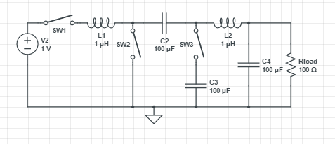
I came across this SMPS topology that I don't recognize. It looks sort of like a combination of a buck converter and a boost converter, but I can't quite figure it out. I haven't been able to find any topologies that match this anywhere. Does anyone know?
-
\$\begingroup\$ A reference to where you found this might be helpfull. C2 and C3 seem superfluous in my opinion if it is really an SMPS. \$\endgroup\$– BimpelrekkieCommented Jun 6, 2016 at 18:46
-
\$\begingroup\$ This looks almost like a "Ćuk". But Ćuk do not have C3. So this may be some variation over Ćuk converter. Where did you get this schematic? \$\endgroup\$– G36Commented Jun 6, 2016 at 18:47
-
\$\begingroup\$ Skipping C3 it is a synchronised Ćuk. Might still be, but I'm too tired/hungry to do the differentials. \$\endgroup\$– AsmyldofCommented Jun 6, 2016 at 18:57
-
\$\begingroup\$ Yes, please provide context for the source of this topology. \$\endgroup\$– user2943160Commented Jun 6, 2016 at 19:19
2 Answers
Not sure what to call the topology, but the circuit appears to be designed to boost a very low voltage at high current to a usable level. A diode drop from a conventional topology represents a large efficiency loss when in the realm of low voltage power sources. You can see from the circuit that the device has a 1-volt input, so its switches have to be timed to turn off and on to direct and block the flow of current to perform a similar function as the diodes would in a topology with high voltage. You can see that if timed properly, the output voltage will be greater than the input, but even a single diode drop in a switcher would drop your efficiency in half or more at one volt input. The output appears to be AC; is this correct?
I don't think this is a SMPS, as it is missing crucial components, and the topology seems off, but it might look similar to a single-ended primary-inductor (SEPIC) converter.
SEPIC converters are often called buck-boost, but in reality they consist of a boost stage followed by a buck-boost stage. They will output a specific voltage over a range of input voltages (even if the input voltage varies over time). Their advantage over conventional buck-boosts are a non-inverting output and true full shutdown with very low quiescent current.
-
\$\begingroup\$ For me this looks more like a "Ćuk" converter. \$\endgroup\$– G36Commented Jun 6, 2016 at 18:53
-
\$\begingroup\$ Those are very similar to a SEPIC converter, but the second stage is a buck instead of buck-boost. Their output is also inverted. \$\endgroup\$ Commented Jun 6, 2016 at 18:56
-
\$\begingroup\$ @G36 is right, the last inductor makes it highly unlikely this offers a non-inverted output. The cap is off-putting, but without it it's just a synchronised Ćuk \$\endgroup\$– AsmyldofCommented Jun 6, 2016 at 18:56
-
\$\begingroup\$ C3 should be a diode in all cases, not sure how the cap made it in there. \$\endgroup\$ Commented Jun 6, 2016 at 18:59
-
\$\begingroup\$ This is definitely a working circuit, I found it in a consumer product exactly as I diagrammed it. \$\endgroup\$– eenoobCommented Jun 6, 2016 at 20:14

