1
\$\begingroup\$

I have designed a BJT based switch to enable and disable one or more loads with a microcontroller pin. The situation is the following:

  • The controller pins work with 3.3V
  • The devices require 12V to work, and a current of 0,85mA flows at this voltage

I put together this circuit: enter image description here

The schematic represents four loads operating together (the four 14,2 KOhm resistors). The idea is to control the NPN with a controller pin. The NPN will, in turn, control the PNP which enable/disable the current flow to the four loads. The Zener guarantees 12 Volts even if one or more loads are missing. The 50KOhm resistor limits the base and collector currents of the NPN, and regulates the emitter-collector current of the PNP. Both BJTs should work in saturation mode.

I simulated this with everycircuit, and it looks ok to me, but I am very newbie in electronics, and I fear I am doing something wrong. So the question is: would such a design work in the real world?

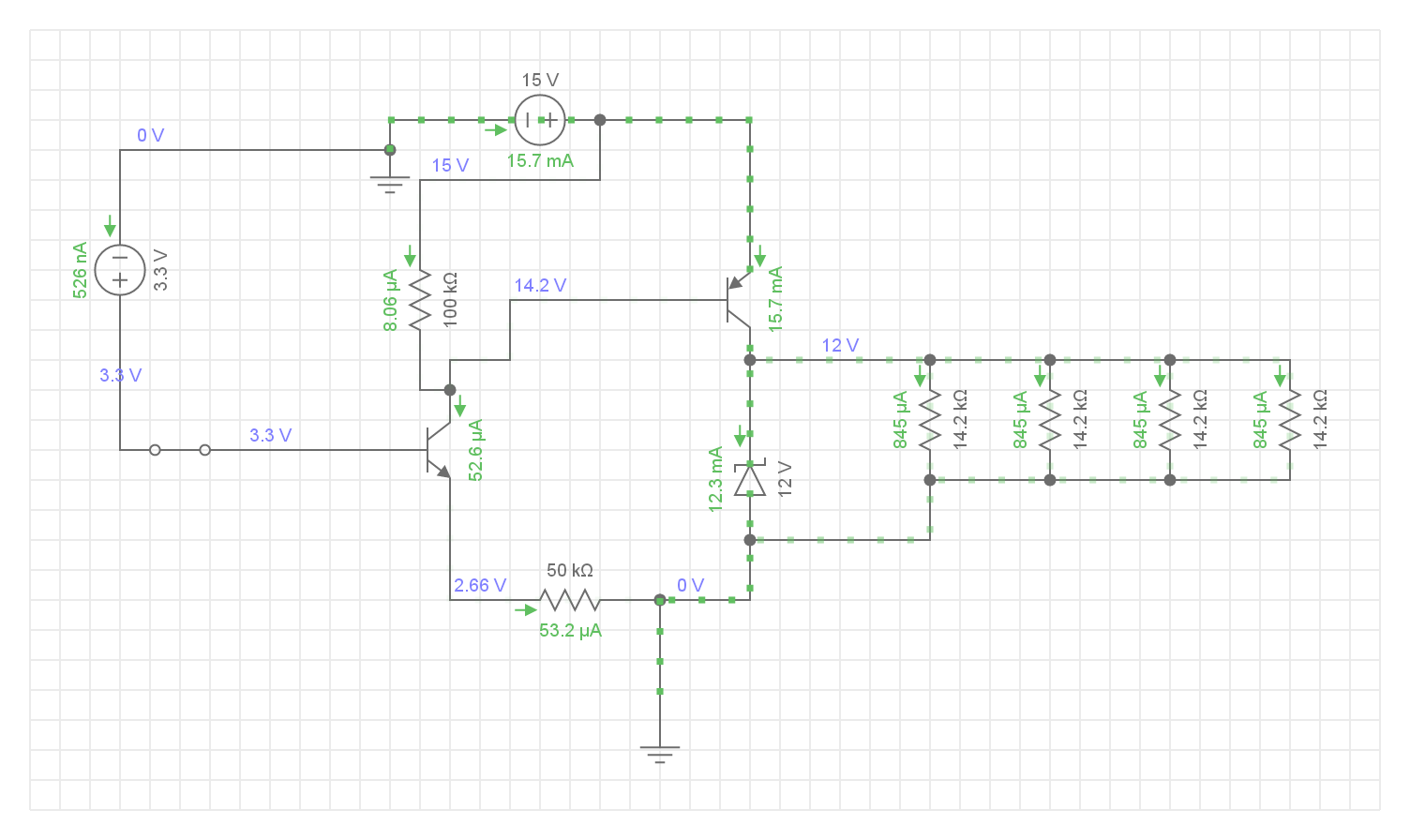
\$\endgroup\$
1
  • 2
    \$\begingroup\$ You can't rely on the PNP beta for limiting the current into the 12V zener. \$\endgroup\$
    – Andy aka
    Commented Jun 16, 2016 at 14:07

2 Answers 2

1
\$\begingroup\$
  1. Here you can find an excellent answer for how to draw a good schematic.

  2. What you are trying to do is called "high-side switching" and good answer / explanation can be found in this answer.

  3. Your Zener diode has no current limiting element and it might blow. As you can see here the differential resistance of the zener diode is very low after reaching the zener voltage. With no current limiting element (resistor) the current through the zener get very high and it might blow. A zener voltage regulator is usually designed like this. Be careful, a zener voltage regulator has usually a quit low output current as the load current is flowing through the zener resistor as well and the resulting voltage drop is cutting of your zener voltage for higher currents.

\$\endgroup\$
1
  • \$\begingroup\$ Thank you for the hints! I found the point one very very interesting. I will edit my question with an updated schematic. Thank you for the information about the zener diodes, I'll apply them in my project. \$\endgroup\$
    – Enrico
    Commented Jun 17, 2016 at 8:13
3
\$\begingroup\$

There are a number problem with your circuit and your schematic:

  1. No component designators. This makes the circuit difficult to talk about.

  2. Those annoying green dots add clutter and make the circuit harder to see.

  3. The layout is really bad. A schematic has to be correct, but good schematics try to help you see the circuit, not make you decipher them first.

  4. The transistor gain assumptions seem to be wildly optimistic, especially since no particular part is called out.

  5. The zener has nothing to work against to limit the voltage. Good transistor circuits work with transistor gain from the minimum guaranteed to infinite. For the zener, the worst case is infinite. Consider the PNP essentially shorting the top end of the zener to the 15 V supply. Something will have to give. A resistor in series with the PNP emitter is one possible solution.

\$\endgroup\$
1
  • \$\begingroup\$ Thank you for your suggestions, I'll refactor the schema and post an updated version. \$\endgroup\$
    – Enrico
    Commented Jun 17, 2016 at 8:14

Your Answer

By clicking “Post Your Answer”, you agree to our terms of service and acknowledge you have read our privacy policy.

Not the answer you're looking for? Browse other questions tagged or ask your own question.