6
\$\begingroup\$

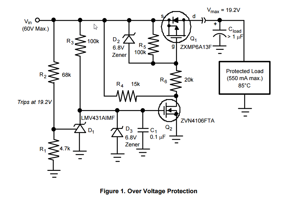
I am unsure what the following statement on page 4 of this application note (Over Voltage Protection Circuit for Automotive Load Dump) means.

Resistor R4 provides a small amount of bias to Q2 in order to satisfy Q2 ’s drain leakage in the off state.

I assume R4 is to satisify Idss in the datasheet of 50uA but I am unsure how the value of R4 was even selected.

Does this mean that all mosfets must have their leakage currents requirements satisfied in order to work ? Why wasn't R5 + R6 not sufficient for this path ?

enter image description here

\$\endgroup\$
3
  • \$\begingroup\$ 50uA of Ids would cause ~5V drop across R5 which would be enough to keep Q1 on permanently, although why they didn't just drop R5 to 10K I've no idea. it's not like it's going to save power or something as R4'll be seeing the full 60V across it when Q2 turns on. \$\endgroup\$
    – Sam
    Commented Jun 24, 2016 at 1:54
  • \$\begingroup\$ I think R5's value needs to be large relative to R6; otherwise with the nominal 12 VDC input (assuming a car battery), Q1's gate voltage will be around 8.25 VDC, its source voltage 12 VDC, and VGS=-4.25 VDC, which (a) does not turn on Zener diode D2, and (b) is probably not enough voltage to drive Q1 into its ohmic region (switched ON). With R5 = 100k, the resistor divider R5 and R6 try to drive Q1 gate to 2.16 VDC, but now Zener diode D2 turns on, locking Q1 VGS=-6.8 VDC, which is (presumably) sufficient to drive Q1 into its ohmic region (switched ON). \$\endgroup\$ Commented Jun 24, 2016 at 3:21
  • \$\begingroup\$ I guess I should've looked at Q1's datasheet before commenting. According to the datasheet Q1's Miller plateau occurs at around VGS=-3.2 VDC; so if VGS=-4.25 VDC this would likely be sufficient to drive Q1 into its ohmic region. However, when Zener diode D2 is conducting (ON) it provides a very low-impedance path between Q1's source and gate, allowing Q1's gate voltage to quickly track Q1's source voltage. Maybe that's what the circuit designer had in mind here. \$\endgroup\$ Commented Jun 24, 2016 at 3:34

2 Answers 2

4
\$\begingroup\$

For Q1 to be off (where 'off' is defined as less than 250uA current) the gate-source voltage must be less than 1V (according to the datasheet value of Vgs(th). Since R5+R6 || R4 = 13.33K, and the gate sees 100/120 of the voltage, up to 90uA of leakage would be acceptable. That's a pretty conservative design considering the leakage is rated at Tj=125°C, unless you have some reason to expect very high operating temperatures (perhaps this is intended to operate in an under-the-hood environment).

If R5+R6 were lowered to 11K/2K it would work similarly, but the zener would see a lot more current at high input voltages. With 60V in, R6 would be dissipating 1.6W vs. 0.24W in R4 plus 0.14W in R6. If you change the ratio of R5/R6 then it affects how much gate voltage is on Q1 with a low input voltage, and you'd have to analyze how that would affect the circuit (perhaps Q1 would burn up during cranking, for example).

\$\endgroup\$
0
\$\begingroup\$

Okay, I ran some PSpice "DC Sweep" simulations on this circuit, sweeping VIN's value from zero volts to 60 VDC, and with the nominal temperature parameter (TNOM) set to 125C. Here's what I found. (Caveat: I substituted an International Rectifier IRF9530N HEXFET Power MOSFET part for transistor Q1 because I couldn't quickly locate a SPICE model for the ZXMP6A13F part and I was too lazy to create that SPICE model from scratch.)

Case 1) Original circuit. For VIN>=8.3V, zener diode D2 is ON and it clamps Q1 VGS=-6.8V over VIN's effective voltage range. (n.b. I'm assuming a 12 VDC car battery is the nominal power source). So as I stated in my second comment in response to @Tom's comment, I think D2's job is to provide a low-impedance path between Q1's source and gate pins, thereby ensuring Q1's gate voltage rapidly tracks Q1's source voltage (i.e., VIN). If D2 were removed there would be an RC time constant between Q1's source and gate that would add unwanted ripple to the DC output voltage at Q1's drain. And finally, for VIN=60V, Q1 VGS≅-40mV.

Case 2) Original circuit, but remove resistor R4. The DC Sweep simulation yielded essentially the same results as for Case 1, except that for VIN=60V, Q1 VGS≅-400mV (roughly 10x its former value). Note that Q1's gate threshold voltage is spec'd as -1.0 VDC <= VTH <= -3.0 VDC. So clearly, R4's job is to hold Q1 VGS well below the -1.0 VDC minimum.

Case 3) Original circuit, but remove resistor R4 and change R5's value to 10k. In this configuration, Q1 VGS never exceeds -6.8 VDC. At approximately VIN=19V, D1 triggers ON, turning OFF Q2, turning OFF Q1 (this occurs before Q1 VGS reaches -6.8V). In other words, zener diode D2 never turns ON, and I would expect to see increased voltage ripple at Q1's drain. And finally, for VIN=60V, Q1 VGS≅-60mV.

\$\endgroup\$
3
  • \$\begingroup\$ +1 It should be noted that SPICE simulation models will use 'typical' values for things like leakage as a function of temperature. Worst-case values should be used for design purposes- SPICE is more-or-less the equivalent of building a circuit to see if one instantiation happens to work. In reality some parts will be worse or better than others, and the parts are only guaranteed to do what is on the datasheet. \$\endgroup\$ Commented Jun 24, 2016 at 14:22
  • \$\begingroup\$ Agreed. To test how Q2's worst case IDSS affects the PSpice circuit simulation, one could set VIN=60VDC, replace Q2 with a 50 uADC current source (IDC), and then run, say, a Bias Point simulation to estimate steady-state Q1 VGS for the three cases mentioned above (or perhaps run a DC sweep of the IDC source). One could additionally assign tolerances to the passive components and run a DC Sweep of VIN in conjunction with a Monte Carlo or Worst Case simulation, and include a Smoke analysis to gain additional insight. These tasks are left as an exercise for the reader. \$\endgroup\$ Commented Jun 24, 2016 at 20:51
  • \$\begingroup\$ The purpose of D2 is protecting Q1 so that the maximum Vgs rating is respected. For Q1, Vgs must be between -20V and +20V. \$\endgroup\$ Commented Aug 31, 2019 at 11:54

Your Answer

By clicking “Post Your Answer”, you agree to our terms of service and acknowledge you have read our privacy policy.

Not the answer you're looking for? Browse other questions tagged or ask your own question.