No, there is not. Well, not for an antenna- You can make a junction with a soldermask opening that will create a short (if you use a stencil cut from the output of the CAM tools), but there's no way to join two different nets on a copper layer in the PCB editor.
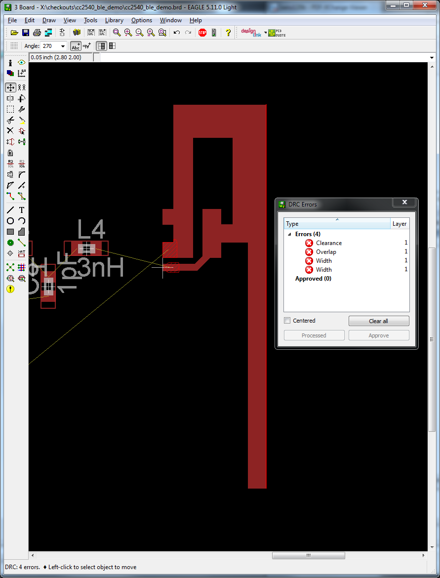
Just keep doing what you're doing; it will produce a DRC error but that's OK.
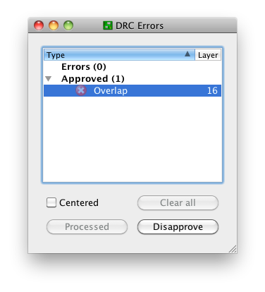
As I wrote at How do I facilitate keeping multiple grounds, (i.e. AGND, DGND, etc…) separated in the layout when using Eagle?, you can move on by select one of the errors to enable the "Processed" and "Approve" buttons ("Approve" is the only one I use on a regular basis) and choosing "Approve" to move the error from the errors list to the approved list:

and will stay there on subsequent runs of the DRC. Note that this only moves this specific error with this specific pair of nets at this specific location. Closing this window and running the DRC again produces the notification "DRC: 1 approved errors"

and no "DRC Errors" dialog. When you don't get a new DRC errors dialog, you're done!


