2
\$\begingroup\$

The Intel D1000 MCU datasheet says:

The MCU has 4 kB of data flash and 32 kB of code flash. Code flash occupies the address range 0x2000 0000 to 0x3FFF FFFF and is aliased throughout. It is accessible from both 128-bit code and 32-bit data busses. Data flash occupies the address range 0x4000 0000 to 0x5FFF FFFF and is aliased throughout.

The size of the address space is:

0x2000 0000 ~ 0x3FFF FFFF = 512M Bytes

0x4000 0000 ~ 0x5FFF FFFF = 512M Bytes

  • But the datasheet says the MCU has only 4kB data flash and 32kB code flash. Why the address space is so big and the physical size is so small? Does it mean that only the first 4kB or 32kB of the big address space can be used?

  • And what does aliased mean?

\$\endgroup\$
1

2 Answers 2

4
\$\begingroup\$

Another word for "aliased" is "duplicated". The same physical memory location can be accessed at multiple locations, all 4K/32K apart.

Basically, they only decode the bottom 12 or 15 address bits (and some top ones for chip select).

As for why? The address registers are 32 bit, but they've only provided tiny storage chips.

\$\endgroup\$
1
0
\$\begingroup\$

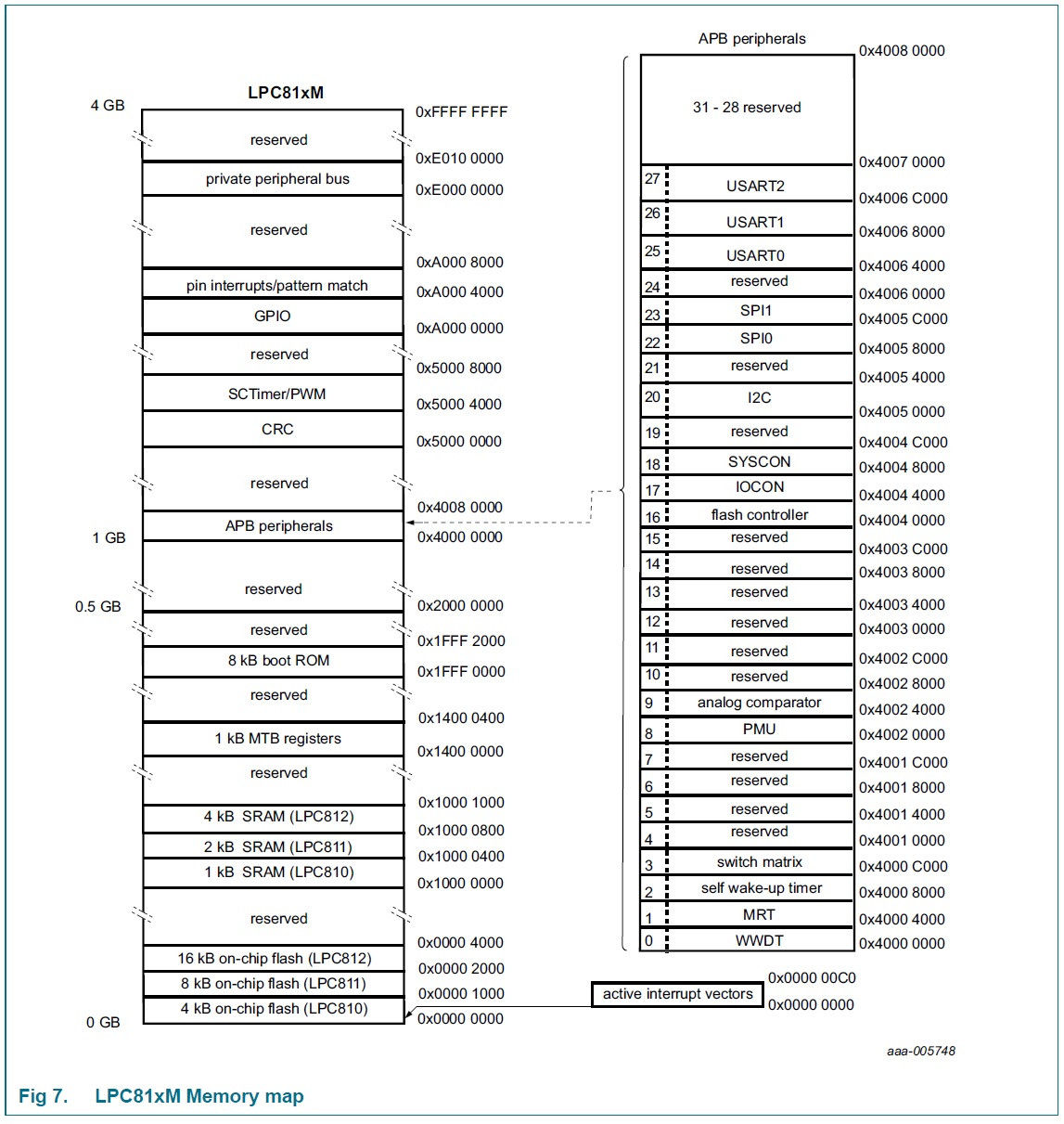
I'm not familiar with this MCU ,but maybe it is reserved for external memory allocation ,Also in some architectures like ARM (vise versa AVR series as i know )there are a unique memory address for all of the memories and peripherals.then this unique memory is used for all peripherals not only for memories. Below is memory mapping of LPC81x cortex m0 from it's datasheet: enter image description here

\$\endgroup\$
1
  • \$\begingroup\$ Thanks. The memory map is critical to understand a MCU. D1000 use memory-map for all registers and peripherals. \$\endgroup\$ Commented Jul 19, 2016 at 2:21

Your Answer

By clicking “Post Your Answer”, you agree to our terms of service and acknowledge you have read our privacy policy.

Not the answer you're looking for? Browse other questions tagged or ask your own question.