1
\$\begingroup\$

I am examining a schematic which concerns the TPS61030 boost converter IC and I have a question regarding the logic behind pulling the enable pin (EN). The schematic is from Adafruit and can be found here: https://learn.adafruit.com/adafruit-powerboost-1000-basic/downloads#schematics

General information:
The TPS61030 boost converter (datasheet) utilizes a signal on its EN pin to turn the converter on or off. If the EN pin is set to 0VDC, the converter is put into shutdown mode which effectively isolates the load from the input. When the EN pin receives an input >= 1VDC (but less than the 7VDC maximum), the device is put into operation mode and starts to function.

The circuit is designed for a 3.7VDC (nominal) LiPo battery. Under ideal conditions, the circuit boosts the 3.7VDC from the battery to ~5.2VDC required by many devices. I believe the +0.2VDC is meant to compensate for low-grade wires.

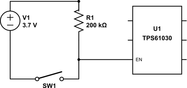
In their diagram, Adafruit pulls the EN pin high and uses a switch to GND to turn the device off. The schematic resembles the following:
schematic

simulate this circuit – Schematic created using CircuitLab

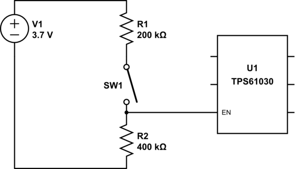
When the switch is open, the converter will enter operate mode. When the switch is closed, the device converter will enter shutdown mode; however, the circuit will become a parasitic drain on the battery. It seems odd to me that the circuit was designed to draw current when the converter, and by extension the device being powered, is meant to be off. I know it will only be ~0.02mA but I do not understand why they wouldn't pull the pin low and use a high side switch instead such as in the following schematic:
schematic

simulate this circuit

The above circuit will form a voltage divider which will output ~2.4VDC to the EN pin which is more than enough to enable the device. When the switch is open, the EN pin will be pulled to GND and the converter will enter shutdown mode. This would eliminate the parasitic drain when the converter is in shutdown mode.

Questions
Why they are pulling the pin high instead of low to eliminate the parasitic drain? I am a novice in electronics so I assume Adafruit has a good reason for doing so and I'm just too inexperienced to understand why. Any input would be greatly appreciated!

\$\endgroup\$
6
  • 1
    \$\begingroup\$ Because the EN pin is internally pulled up inside the chip? It's not specified in the datasheet, but it is common for that to be the case. \$\endgroup\$
    – Majenko
    Commented Aug 24, 2016 at 23:01
  • 1
    \$\begingroup\$ Also it is more common to want the device running than not, so why not have that the default? \$\endgroup\$
    – Majenko
    Commented Aug 24, 2016 at 23:03
  • \$\begingroup\$ @Majenko Thanks for the response. In my application, the device will be off for relatively long periods of time, sometimes for a few weeks before being turned back on. \$\endgroup\$
    – John P.
    Commented Aug 24, 2016 at 23:10
  • 1
    \$\begingroup\$ My guess is that Adafruit wants people who bought the module and connected a power input for it to just work. Think about the hassle of technical support to people who didn't realize to short out or connect a switch to EN if done the other way. (And 20uA is not much current although not negligible for an 1Ah battery for example.) By the way, the best way to minimize the power-off power is to put the switch between the battery and the module. That eliminates any current that the circuit might drawn when in shutdown mode. \$\endgroup\$
    – rioraxe
    Commented Aug 24, 2016 at 23:40
  • \$\begingroup\$ @rioraxe Great point, I didn't even think about that aspect of it. \$\endgroup\$
    – John P.
    Commented Aug 25, 2016 at 1:38

3 Answers 3

3
\$\begingroup\$

Possible reasons: part count, reliability, lack of concerned about that that level of leakage, avoiding complexity, default-on behavior for user convenience (from rioraxe in the question's comments).

To expand on leakage current being of little concern: check the specification of the TPS61030: 20uA (typ). Then 1uA (max) in shutdown. What will another 20uA of leakage through the pull-up do? Expanding on laptop2d's calculations: 21uA leakage from a 1000mAh battery gives 47,600 hours of "standby" time (discounting battery self-discharge). Over 5.5 years! The self-discharge of the attached secondary cell and the usage of the device are certainly of greater power-loss concern than shutdown leakage! Leaving shutdown then trades pull-up current for the converter's quiescent current.

Thus, the expected use of this board is not greatly concerned about leakage currents in comparison to the 100 to 1000+ mA loads the battery will see in normal operation (e.g. phone charging, running an rPi).

If you were using this for something other than a USB power bank, you might be concerned about battery life. However, long-lifetime battery operated devices usually don't come equipped with 4A-switch boost converters.

Note: the proposed 200k pull-up and 400k pull-down with switch circuit would not work. From the datasheet, The device is put into operation when EN is set high. It is put into a shutdown mode when EN is set to GND. This looks to be a normal logic input, so it is intended to be driven close to the rails. It is not a comparator input like the LBO pin or certain other regulators that have precision-threshold enable inputs.

\$\endgroup\$
5
  • 1
    \$\begingroup\$ Additionally: don't necessarily expect that Adafruit (or any "maker" branded vendor) has the best reason behind their design decisions. For personal example, I noticed that the Adafruit TMP006 breakout does not (ca. 2014) follow TI's recommended layout, which could affect its accuracy. \$\endgroup\$ Commented Aug 24, 2016 at 23:17
  • \$\begingroup\$ Thank you for the informative answer. Like I was telling laptop2d, my battery is a 10.2Ah LiPo pack. I'm honestly not concerned with the draw itself, the battery will most likely stop working from age before the current drains it. The purpose of my question is to understand the logic of choosing one circuit over the other. My co-worker said it may be to save money on the second resistor but I assumed it was more complex than that. \$\endgroup\$
    – John P.
    Commented Aug 24, 2016 at 23:24
  • \$\begingroup\$ I was just going with the nominal value that laptop2d used to have our calculations be easy to compare. I'll update my answer a bit. \$\endgroup\$ Commented Aug 24, 2016 at 23:43
  • \$\begingroup\$ Thanks for the added information. I was confusing two datasheets I'm working with. Converter TPS61230 implies the EN pin can be triggered at 1.2VDC whereas this converter specifies 0.8 x VCC. If I modify the R1 value to be 100k and R2 to be 600k, I can get above 0.8 x VCC which I assume will enable it. \$\endgroup\$
    – John P.
    Commented Aug 25, 2016 at 1:36
  • 1
    \$\begingroup\$ Maybe, but making the node too high impedance could also make it sensitive to coupled noise. If anything, considering a multiple-resistor for the enable divider is an over-optimization of the design. \$\endgroup\$ Commented Aug 25, 2016 at 1:43
1
\$\begingroup\$

Will it become a parasitic drain? Depends on the definition of parasitic. The answer is read the datasheet again and again, if you don't understand something look it up.

From the datasheet: Shutdown current VEN= 0 V, VBAT = 2.4 V Current of enable pin = 0.1 to 1 μA

1uA of current from a 1000mA*H battery will last you 1e6 hours, I hope thats enough for you. And the pin varies from part to part or is dependent on the voltage so it could even be lower than 1uA. Thats why we love FET's

A bigger worry than the enable pin is the part itself, it has 25uA of Quiescent current. That's only ~38k hours on the same 1000mA*H battery.

A better way to handle this in your schematic is have your entire device switched from the battery if possible and tie the enable to Vbat.

\$\endgroup\$
1
  • \$\begingroup\$ Thanks for the response. In the first diagram, the switch being closed turns the device off. This makes current flow through R1 to ground. Ignoring the small current draw of the EN pin completely, the small current through R1 will draw current from the battery. I'm not exactly concerned with the drain itself, I'm using a 10.2Ah battery. I'm concerned with the logic of choosing one circuit over the other. A co-worker said it may be to save money by using one resistor instead of two. For the purposes of learning, let's assume I cannot switch the entire part. \$\endgroup\$
    – John P.
    Commented Aug 24, 2016 at 23:19
0
\$\begingroup\$
  • Actually looking at this again, they are using it as a pull-down and the resistor is simply a load resistance so as not to have a dead-short.

Disregard: So this may not be the entire concept, as I haven't had a chance to look at the datasheet in detail, but you've pretty much addressed it with your insight about the voltage divider acting in the same way.

You could use this 400ohm resistor as a current limiting resistor, but the voltage drop is undesirable and this may change the "loading" of this pin when the switch is closed. Given that this is looking at a voltage, I'll assume it's a very high impedance so this would prob be negligible, but it should be noted that this will add resistance to ground which can cause looping issues.

The job of a pull-up is to ensure that the voltage level is correct when switched, this seemingly being an "active low" you want to make sure that it stops in good time, so pull-up, flip the logic and you may need a pull-down. In both of your configurations the resistors are acting as pull-ups, just one is a stiff voltage divider which can introduce a ground differential.

\$\endgroup\$

Your Answer

By clicking “Post Your Answer”, you agree to our terms of service and acknowledge you have read our privacy policy.

Not the answer you're looking for? Browse other questions tagged or ask your own question.