1
\$\begingroup\$

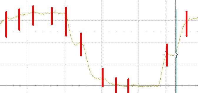
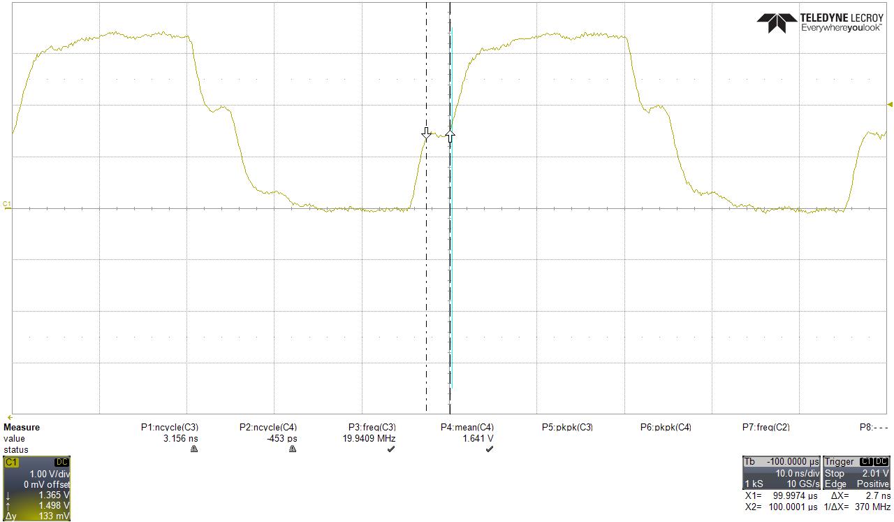
I'm trying to debug a clock signal between two ICs (DS90CR287 and DS90CR288). There is a step half way up the single ended clock generated by the DS90CR288 which I don't know how to explain. I can't post the schematic but there is a 30Ohm series resistor between the output clock (DS90CR288) and input clock (DS90CR287).

Oscilloscope capture of clock

EDIT

I meant to say between two DS90CR287 ICs and a DS90CR288. It seems like the cause of the step is using series termination rather than parallel termination.

\$\endgroup\$
7
  • 2
    \$\begingroup\$ looks like reflection to me, what amplitude is it supposed to be into what load and howis the tracks laid out etc.? \$\endgroup\$
    – PlasmaHH
    Commented Sep 20, 2016 at 13:52
  • \$\begingroup\$ Given the length of the step, it looks like a reflection in 300+ mm cable (a scope probe?). Try measuring with a 10X attenuated probe. \$\endgroup\$ Commented Sep 20, 2016 at 14:43
  • 1
    \$\begingroup\$ Let me guess - you missed the part of the data sheet circuit which shows termination resistors on the inputs of the 288, right? \$\endgroup\$ Commented Sep 20, 2016 at 14:44
  • 1
    \$\begingroup\$ @DmitryGrigoryev I switched from an active probe to a 10x probe and the reflection is still there although slightly less pronounced \$\endgroup\$
    – ks0ze
    Commented Sep 20, 2016 at 15:17
  • 1
    \$\begingroup\$ @WhatRoughBeast you're talking about the 100 Ohm across the LVDS pairs, right? Those termination resistors are there. Where I'm seeing the problem is on the LVTTL output of the 288. \$\endgroup\$
    – ks0ze
    Commented Sep 20, 2016 at 15:25

2 Answers 2

1
\$\begingroup\$

Let me offer an analysis of the presented trace.

This is a classic high-speed waveform when a probe is placed at the source of clock that drives a trace (or transmission line, or coax cable) with no termination on the destination end. The driver impedance (plus any in-series resistor) forms a voltage divider with the line impedance (which is 103 Ohms, as reported). The initial voltage amplitude gets divided in Driver/Zline proportion. Then the signal propagates to unterminated end, and is 100% reflected, so the DC amplitude becomes equal to the driver output amplitude when the reflection comes back.

The duration of "shoulder" is two flight times across the trace. If it is 2.7 ns, it means the one-way flight of 1350 ps. With typical propagation delay of 150 ps per inch, it makes the trace length between two chips of about 200-250 mm.

If the driver impedance matches the transmission line characteristic impedance, the shoulder should be exactly half-way. If the impedances do not match at the source, secondary reflections will occur, making the waveform less pretty. The shoulder on the scope capture is less than half of the DC level, meaning that the driver impedance (driver+resistor) is MORE than 100 Ohms, and the resistor should be reduced or removed.

This shoulder shouldn't be of much concern, because at the destination point the clock will look just fine, and the receiving IC will function just fine as well.

\$\endgroup\$
2
  • \$\begingroup\$ Upvote to neutralize drive-by downvote without comment. Plus interesting that this might be an artifact of reflection! \$\endgroup\$
    – Araho
    Commented Aug 8, 2017 at 6:04
  • \$\begingroup\$ Learned something! :) +1 \$\endgroup\$
    – user98663
    Commented Aug 8, 2017 at 9:59
1
\$\begingroup\$

Most likely it is measurement error from improper test methods.

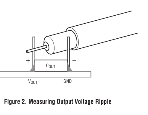
The signal captured is a 20MHz square wave with a resonant signal near 200MHz which could be the 9th harmonic at 180Mhz due to probe inductance rather than a balanced low ESL probe method with very short or no ground wires, just using a calibrated 200MHz probe tip & Barrel with matched source and load.

You could be getting textbook waveforms if you follow best practices for signal integrity, supply decoupling and signal capturing. It is possible to get < 0.1% noise or 60dB SNR. Yours is about 16 dB SNR. tisk.

enter image description here

get spring probe accessory or make this happen then show new photo.

No need for cap shown in photo, that's for Supply Voltage ripple into an AC coupled 50 Ohm termination.

enter image description here

  • your lab instructor or mentor ought to know better. Now you do.
\$\endgroup\$
2
  • 1
    \$\begingroup\$ I am sorry Tony, but this is a classic waveform at the driver of a 25 cm unterminated transmission line. \$\endgroup\$ Commented Jul 3, 2017 at 2:50
  • \$\begingroup\$ Good call. agreed. 3.3V signal is definitely unterminated. With 100 ohm differential I see spec is Vos=1.25V (CM) and Vod = 0.29V typ and 0.45 max for Differential Output Voltage RL = 100Ω . certainly not 0 ~3.5V although there is some probe ringing from test method error, design error is the main reason. \$\endgroup\$
    – D.A.S.
    Commented Aug 8, 2017 at 6:23

Your Answer

By clicking “Post Your Answer”, you agree to our terms of service and acknowledge you have read our privacy policy.

Not the answer you're looking for? Browse other questions tagged or ask your own question.