I've got a board with two Altera CPLDs on it with a bit of a programming problem: programming it via JTAG fails.
The JTAG lines run through the first board, through a flex, and a few emerge on the other board underneath some other components. The rest seem to emerge under the CPLDs, which are on top of each other, or back to back for want of a better way of explaining it.
I don't know whether the JTAG lines run parallel all the way, nor do I know what order the tracks are in inside the board - hopefully TDO is away from TCK... The board has at least 4 layers from what I can tell.
When I go to program the device, I can run the "Detect JTAG chain info" utility in MAX+plus II. It returns a message saying "JTAG chain information confirmed by hardware check", which is good. Then, I can run a blank check, which fails.
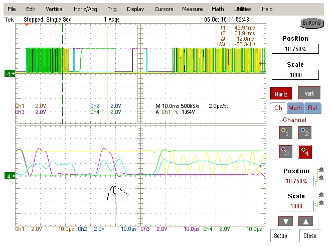
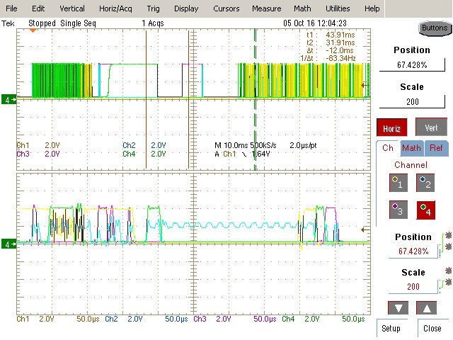
If I disconnect TDO at the JTAG header and run a piece of wire to the JTAG pins on one of the CPLDs, it works. The data looks mostly fine on the oscilloscope with pretty sharp edges and minimal ringing. However, I get some spurious oscillations at certain points when I probe it:
The traces are as follows:
Yellow: TDO
Cyan: TCK
Magenta: TMS
Green: TDI
You will notice that TCK never quite makes it to the rail occasionally. When it does, it is very sinusoidal and not at all square.
TDO only oscillates when TDI is high, but not every time TDI is high. TCK seems to oscillate when TMS rises with TCK or when TDI rises with TCK.
I'm using a Bitblaster and have fitted a 1 kΩ resistor between TCK and ground and the remaining three lines have a 1 kΩ resistor to Vcc.
The scope screenshots were taken with TDO routed through a piece of wire straight to the CPLD. I've tried doing this with TCK and the waveforms still have this noise on them. If I try doing the blank check again without changing anything, the noisy bits move around.
Does anyone have any ideas as to why TCK seems to not make it up to the rail, or why TCK and TDO seem to oscillate?


