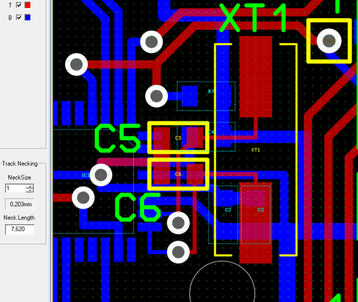
I'm trying to redesign the layout with a 8 MHz crystal(XT1) for atmega328p micro controller. Since this micro controller uses internal oscillator,UART Communication does not work reliably on current design.So I decided to go with external crystal for the production.
Since this board works fine with all the other functionalities except UART,we need to re spin the board with minimal changes.The red represents the top PCB layer and blue is the bottom PCB layer (it's a 2-layer design).Due to the placement constraints on the bottom side of the PCB,I placed the Crystal and its Load capacitance on the Top side whereas the micro-controller sits on the bottom side.
I've been reading through several recommendations specifically for crystals layout design.I am sure that design does not meet most of them(ex.Avoid vias). I am concerned about the functionality of the PCB, especially from EMC problems.There are really no high frequency signals on this board except 8 MHz . Can anybody give some suggestions on how the PCB can be improved?
