Unless otherwise specified in a CMOS datasheet, and the system design power down dv/dt and monotonicity is guaranteed and the possibility of EMI during shutdown is "totally immune" , then there is no chance of predicting the output transition activity when Vcc is below specified operation.
In order to appreciate this, you must understand that ALL logic devices are linear amplifiers that saturate and switch quickly. This means the when internal Vgs crosses the threshold it becomes a pure linear amplifier with a very high gain of any ripple on the input. At his point during Vcc decline the RdsOn of each FET is also rising making it less immune to stray noise.
Unlesss you test every supplier under all conditions, it would be impossible to generalize any safe shutdown condition.
example in industry
Because of this uncertainty during power down ( controlled or otherwise) ALL Winchester disk drives since the original designs had a write disable signal right on the R/W chip inside the head-arm assembly that abruptly shut off write current under any fault condition such as under-voltage to prevent corrupt data write to non-volatile media. I have confirmed this design aspect in dozens of products.
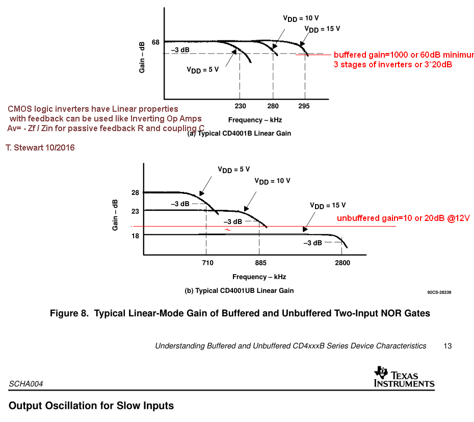
I hav e long said in this forum that all CMOS unbuffered inverters have a gain of >10 and buffered inverters have have a gain of >1000 in linear operation,
This is the characteristic of CD4xxx and 74HCxxx family logic. aka High V CMOS or HC.
It is my understanding that although there are over 50 variations of CMOS logic thresholds with different speed and current limits, the linear gain characteristic has not changed, although I have not verified every family. (e.g. 74ALCxxx , ARM's etc.
I found this current TI document to support my experience since 1974, to show you the linear gain which is the same output stage used in all CMOS of the same CD4xxx/74HC family.

In conclusion you have found one instance where you have a controlled shutdown. But this has many unknowns for EMI immunity and decaying Vcc ripple during shutdown.

