5
\$\begingroup\$

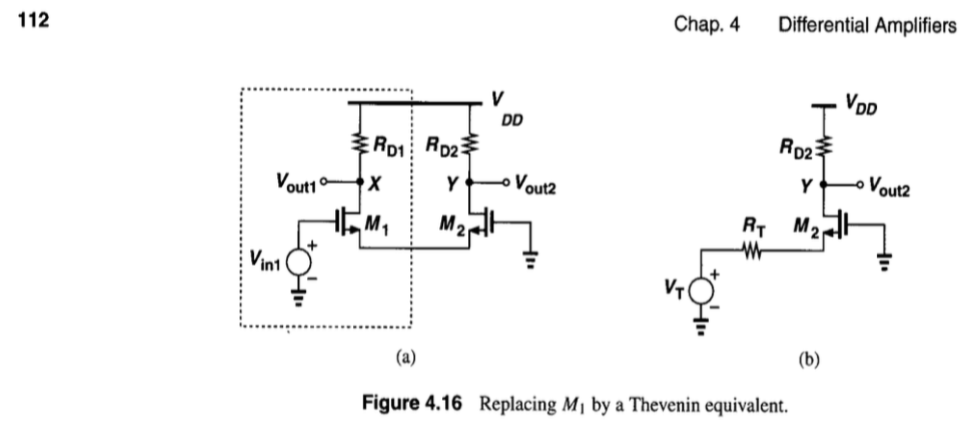
enter image description here I was reading my textbook(razavi) and came across this circuit where to calculate vout2/vin1 he drew a thevenin equivalent of nmos. I dont understand how thevenin voltage(Vt) and Rt in the equivalent circuit is Vin1 and 1/gm1??

The procedure for calculating thevenin was to zero out independent sources and then calculate R across the 2 terminals across which you wanna find. Here if we zero out vin1 we will be in a situation where mos will be off, right? also how Vt calculated to be Vin1?

How can thevenin theorem be appliied to mosfets??

texbook is cmos analog circuit design by razavi.

\$\endgroup\$
1
  • \$\begingroup\$ Nice question ! Razavi has a lot of such small details which looks simple but could be complex as this ! \$\endgroup\$ Commented Feb 19, 2017 at 23:45

4 Answers 4

1
\$\begingroup\$

Since we are trying to find the Thevenin impedance, we would have to compute the impedance looking from the load , in this case I think that it would be from the source of M1 (considering your final equivalent circuit) . So looking from Source of M1 if you draw the small signal model and derive you would obtain an impedance approximately 1/gm1 [ 1 ] .

If you draw the small signal model for the circuit in the left side, you would get something like this,

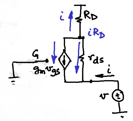
MOSFET small signal resistance from the source

And further using KCL and KVL you will realize that v/i = (Rd + rds) / (1+ gm1*rds1) = 1/gm1 (approximatelly considering Rd = 0). So therfore this explains the 1/gm1 part.

Here if we zero out vin1 we will be in a situation where mos will be off, right?

Remember that the MOSFET is not necessarily off if Vin =0 because to turn on the MOSFET we require a Vgs=Vg-Vs>= Vt and if Vg=0 then Vs can be >= -Vt, thereby turning the MOSFET on.

And for the thevenin voltage I am also not very sure but I think it could be something like this, since to find the Thevenin voltage we will have to remove the load which in this case would be the right hand part of the circuit we would be having only the left hand part with the source of M1 hanging (unconnected or high impedance). Since no current flows through the left hand side Vgs cannot be more than Vt because if it is so, then some current should flow ! So to satisfy this criteria if you assume Vs = Vin then Vgs = 0 therby satisfying the no current condition.

[ 1 ] http://web.iitd.ac.in/~shouri/eel782/lectures.php, refer to the input resistance section (the image is also from the same link).

\$\endgroup\$
1
\$\begingroup\$

Although it might have been apparent from the other answers already posted here, I feel the need to state it explicitly:

Razavi is showing the AC-equivalent circuit

But he is making it rather confusing by using actual transistor symbols... Remember, an AC equivalent circuit uses the biasing as the new origin, effectively making all bias voltages and currents 0V or 0A. If we then perturb the circuit with very small signals, we can linearize all the nonlinear components, such as the mosfets.

This means that the biasing current source at the bottom is left out (it becomes a current source of 0A in AC, which is effectively an open connection). This also means that the necessary voltage \$v_{GS}>V_T\$ is subtracted from the biasing condition making it an AC voltage source centered around 0V!

Finding the Thevenin Equivalent can be calculated (as already mentioned) but can also be seen as follows if you have a bit more background in the field:

The series resistance \$R_T\$ is the resistance seen at the source of M1. You may have learned already that if you look into the source of a transistor, that you will find a conductance of approximately \$g_m\$. And so the Thevenin resistance is then \$R_T=\frac{1}{g_m}\$.

The voltage \$V_T\$ is the voltage you get if there is no load connected to the source of M1. In that case, the circuit to replace can be treated as a source follower. You may have learned already that a source follower will have a gain of 1, so the voltage \$V_{in1}\$ is copied to the output. And so the Thevenin voltage is then \$V_T=V_{in1}\$.

\$\endgroup\$
2
  • \$\begingroup\$ It's a matter of opinions :) I love the Razavi's way: even AC-equivalents are much clearer if not messed up with dependents generators and stuff. Once the three basic (CS, CD and CG) connections impedances and gains are known Razavi's is just plain sailing. \$\endgroup\$
    – carloc
    Commented Jan 14, 2018 at 9:58
  • \$\begingroup\$ I agree, it does make more sense if you're used to it. But op seems to have confused the two... \$\endgroup\$
    – Sven B
    Commented Jan 14, 2018 at 11:09
1
\$\begingroup\$

Here if we zero out vin1 we will be in a situation where mos will be off, right?

As others have mentioned, Razavi is finding the Thevenin equivalent of the circuit using the small signal (ac) model of the transistor (not explicitly drawn in the text). This means we've already assumed the transistor is operating in the saturation region, and all bias voltage and current sources are zero. Thus, \$V_{in1}\$ represents small ac variations, and zeroing it will not put the transistor in the cutoff region.

I dont understand how thevenin voltage(Vt) and Rt in the equivalent circuit is Vin1 and 1/gm1?

Thevenin Impedance

To find the Thevenin impedance we start by drawing the small signal model of the isolated network in the dotted box [Fig. 4.16(a)] (assuming \$\lambda=\gamma=0\$). Notice that we've removed all independent sources (just \$V_{in1}\$ in this case) and inserted a test voltage source \$v_{test}\$ at the load:
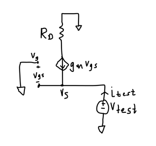
small signal model for calculation of Rth

From the equivalent model, we can write \$v_{gs}=-v_{test}\$ and \$g_mv_{gs}=-g_mv_{test}\$. Next, we observe that \$i_{test}=-(-g_mv_{test})\$. Thus, \$R_t=\frac{v_{test}}{i_{test}}=\frac{1}{g_m}\$. Note that this resistance does not depend on \$R_d;\$ as Sven B mentioned, if you look into the source of a transistor you'll find a conductance of approximately \$g_m\$.

Thevenin Voltage

To find the thevenin voltage we've drawn the same circuit using the transistor small signal model, except we've included the independent sources (just \$V_{in1}\$) and disconnected the load:
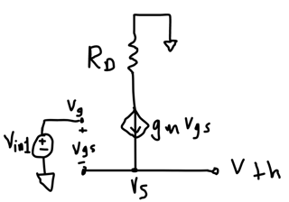
small signal model for calculation of Vth

Because the load has been disconnected, no current can flow through the dependent current source, so \$g_mv_{gs}\$ must be equal to zero. In order for this to be true, either \$g_m\$ or \$v_{gs}\$ must be zero. Because we've assumed the transistor is operating in the saturation region, \$g_m\$ cannot be zero; thus \$v_{gs}=0\$, and \$V_{t}=V_{in1}\$. Sven B pointed out that you can also view this as a source follower, which gives a gain of 1, and \$V_{t}=V_{in1}\$.

How can thevenin theorem be appliied to mosfets??

As long as you are modeling transistors with linear elements (e.g. small signal model), you can apply Thevenin's Theorem to any network of transistors.
\$\endgroup\$
2
  • 1
    \$\begingroup\$ For calculating Thevenin resistance, you are assuming too much. No need to assume Rd << 1/gm at all and that doesn't apply in many cases. \$\endgroup\$
    – emnha
    Commented Mar 13, 2018 at 5:22
  • 1
    \$\begingroup\$ @anhnha You're right. I've updated my answer to include \$R_d\$. \$\endgroup\$
    – Ralph
    Commented Mar 13, 2018 at 5:54
0
\$\begingroup\$

Why we use Thevenin Equivalent Circuit? In order to simplify circuit to only two elements (resistor and voltage supply). Right?

How We Calculate

First find the voltage between two nodes. Then find the resistance between two nodes.

Voltage already known: Vin1

Resistance of Mosfet is 1/gm1. gm1 is called transconductance (electrical characteristic relating the current through the output of a device to the voltage across the input of a device).

\$\endgroup\$
1
  • \$\begingroup\$ Did you cut your answer off in the middle? This looks rather...half-baked to me m8 \$\endgroup\$ Commented Dec 4, 2016 at 22:27

Your Answer

By clicking “Post Your Answer”, you agree to our terms of service and acknowledge you have read our privacy policy.