1
\$\begingroup\$

I'm trying to figure out the flash memory map of ATmega328P:

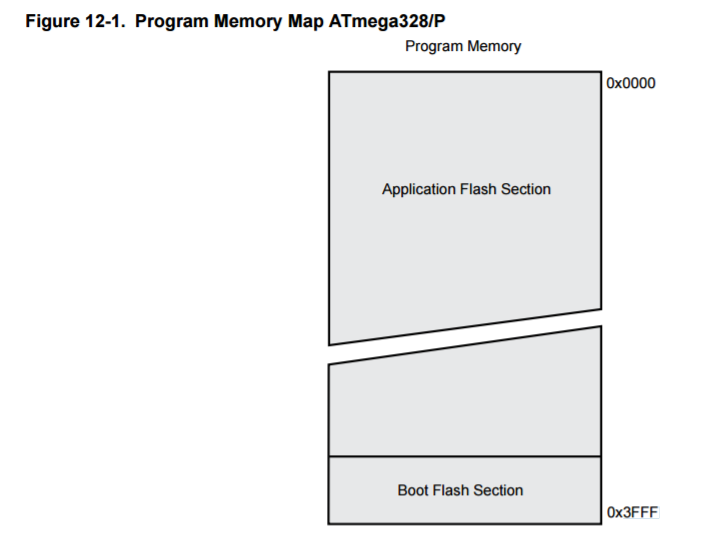
Below is from the datasheet:

enter image description here

Program Memory Map for ATmega328P is given as 32KB: 32Kbytes = 32K * bytes

0x0000 means 16 bit wide (for each line of memory there is 2 bytes)

which is 16K * 16bit

What I understand from this, the flash memory is made up of 16K lines of 16 bit wide registers. So for an instruction on the flash memory the maximum address number is 16K.

Is this 16K 2^16 or 16000?

The last three X Y Z general purpose registers which are used for holding the addresses(pointers) are 16-bit which can store up to 2^16 = 65536 addresses. So I would guess 16K means 65536 here?

But if it is, in the above figure it shows the last memory line as 0x3FFF which corresponds to 16383.

What am I knowing wrong here?

\$\endgroup\$

3 Answers 3

1
\$\begingroup\$

What you are knowing wrong are a couple of things.

Not all AVR devices have the same amount of actual available on-chip program memory. Some may have 8K bytes, 16K bytes, 32K bytes or even 64K bytes. Yours happens to have the advertised 32K bytes.

The X, Y and Z registers are 16-bits wide. These are generically designed to support a data memory map up to 64K bytes. Once again the size of available data memory can vary from device to device type so the whole 64K byte addressability may not be used on all devices.

The X, Y and Z registers are generically indicated right in the data sheet description to be used for accessing data memory. Data memory is not to be confused with program memory. The Z register can be used, in conjunction with certain specific opcodes, to access tables in the program memory (Z still 16-bits to support up to a generic 64K bytes even though the program memory available may be less).

\$\endgroup\$
7
  • \$\begingroup\$ LPM/ELPM/SPM, which access program memory, are intended to be used with Z. \$\endgroup\$ Commented Dec 10, 2016 at 17:26
  • \$\begingroup\$ I know. I was just going to add that to my answer. \$\endgroup\$ Commented Dec 10, 2016 at 17:29
  • 1
    \$\begingroup\$ But data memory is far less than the 16K adress program memory it is only 2KB. X Y Z needed for that 2048 addresses?? \$\endgroup\$
    – user16307
    Commented Dec 10, 2016 at 17:31
  • \$\begingroup\$ Whille it doesn't require 16 bits to address 2KB, it is convenient to have all registers either 8 or 16 bits long - things would get messy if the registers were trimmed to the minimum size required. If the X, Y and Z registers are 16 bits, they can be used for many other things than just addressing RAM. \$\endgroup\$ Commented Dec 10, 2016 at 18:15
  • \$\begingroup\$ "The X, Y and Z registers are generically indicated right in the data sheet description to be used for accessing data memory." I don't get that: Imagine the processor wants to store the last address number(by pointer) of the flash/program memory which is 16383 to one of its general purpose registers. You say 16 bit X Y Z will only hold data about SRAM. The rest of general purpose CPU registers are 8 bit wide. The max number they can hold is 2^8 which is 256. Where will the number 16383 be stored in CPU registers in that case? \$\endgroup\$
    – user16307
    Commented Dec 10, 2016 at 23:09
1
\$\begingroup\$

Is this 16K 2^16 or 16000?

... Neither.

It is 16 * 1024 = 16384.

\$\endgroup\$
0
\$\begingroup\$

The Atmega328 has 32kbytes of Flash memory (program memory). The instructions in the AVR family are 16bits wide, so the flash memory is 32 bytes/2 =16 k words 16kwords= 16*1024 words=16384 memory locations from 0000-3FFF(16 bits wide)

\$\endgroup\$

Your Answer

By clicking “Post Your Answer”, you agree to our terms of service and acknowledge you have read our privacy policy.

Not the answer you're looking for? Browse other questions tagged or ask your own question.