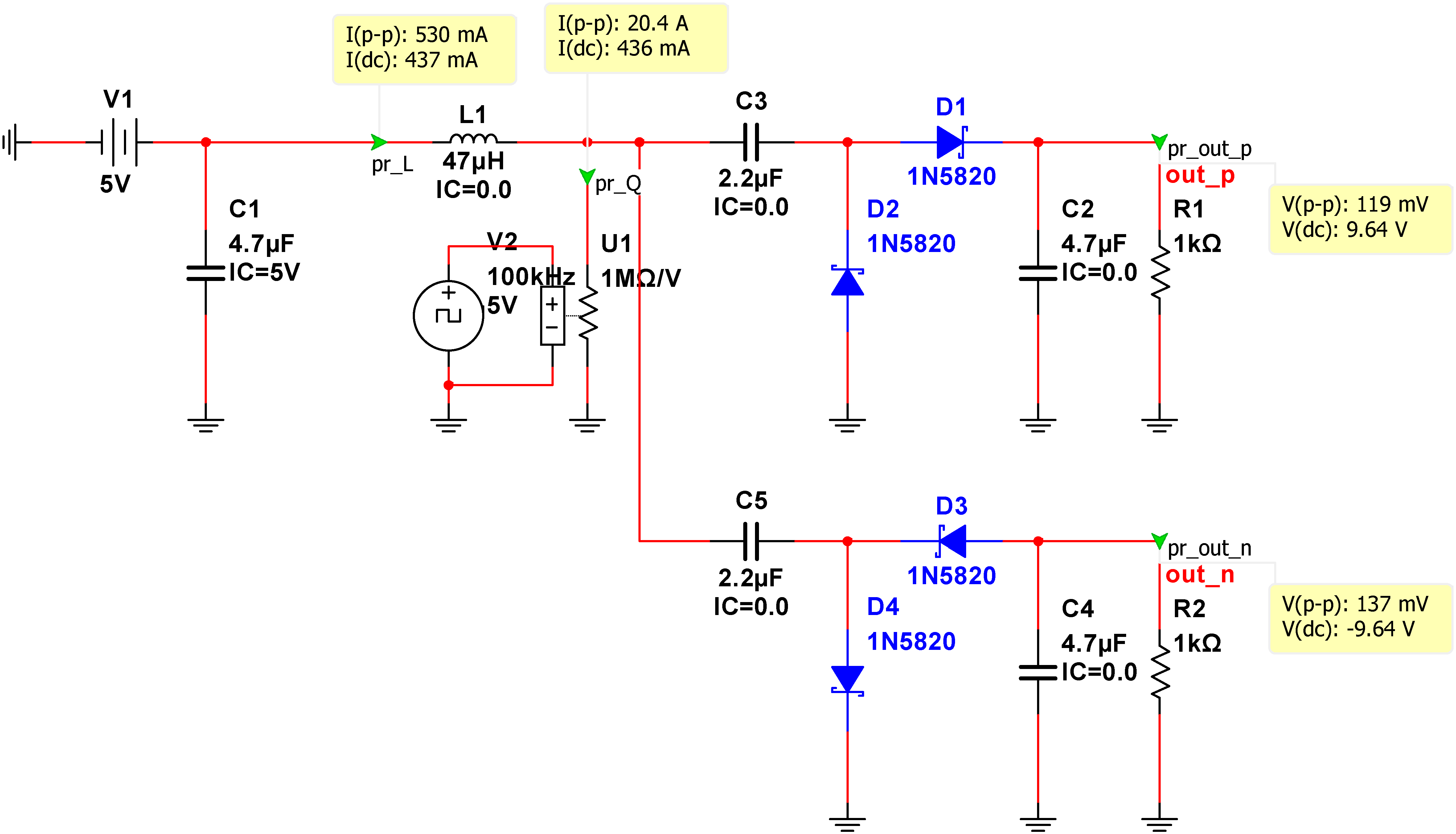
I spotted a circuit in the wild that generates symmetric (e.g. ±8 V) analog power rails from a single +5 V supply using a single boost converter and a single 10 μH inductor. This is a very common use case so I spent some time to reverse engineer it. The following is a schematics/simulation I made:

(source: imgh.us)
U1 and V2 are my make-shift PWM power switch for simulation --- in the actual circuit the net is tied to the SW pin. Of course the positive output is regulated through feedback, but the negative output is not directly tied anywhere.
I found a post by Linear Technology that briefly mentions the negative branch of this circuit as a "inverting charge pump" (Fig. 4), but I cannot find other sources on this topology. The positive branch seems to be just flipping the direction of the two diodes, making it slightly different from the original boost topology...
So what is this really? And what are some advantages/disadvantages of this design compared to e.g.:
- Separate boost and inverting converters (e.g. TPS65131 which integrates both), which requires 2 inductors
- Boost converter followed by a fly-back-capacitor-type inverting charge pump
2017-03-19 EDIT:
After some digging I found this these links:
- Simplest possible 5V to +/- 10-15V converter (for op-amps)
- Inverting charge pump with boost converter loading characteristics
- http://www.ti.com/lit/an/slua288/slua288.pdf
- https://obsoletetechnology.wordpress.com/projects/studio-electronics/dc-dc-bipolar-power-supply-for-effect-pedals/
As I expected this is a very common use case. I think at this point I just need a textbook or equally authoritative source that documents the fundamentals of this topology. Any suggestions?
