-2
\$\begingroup\$

enter image description here

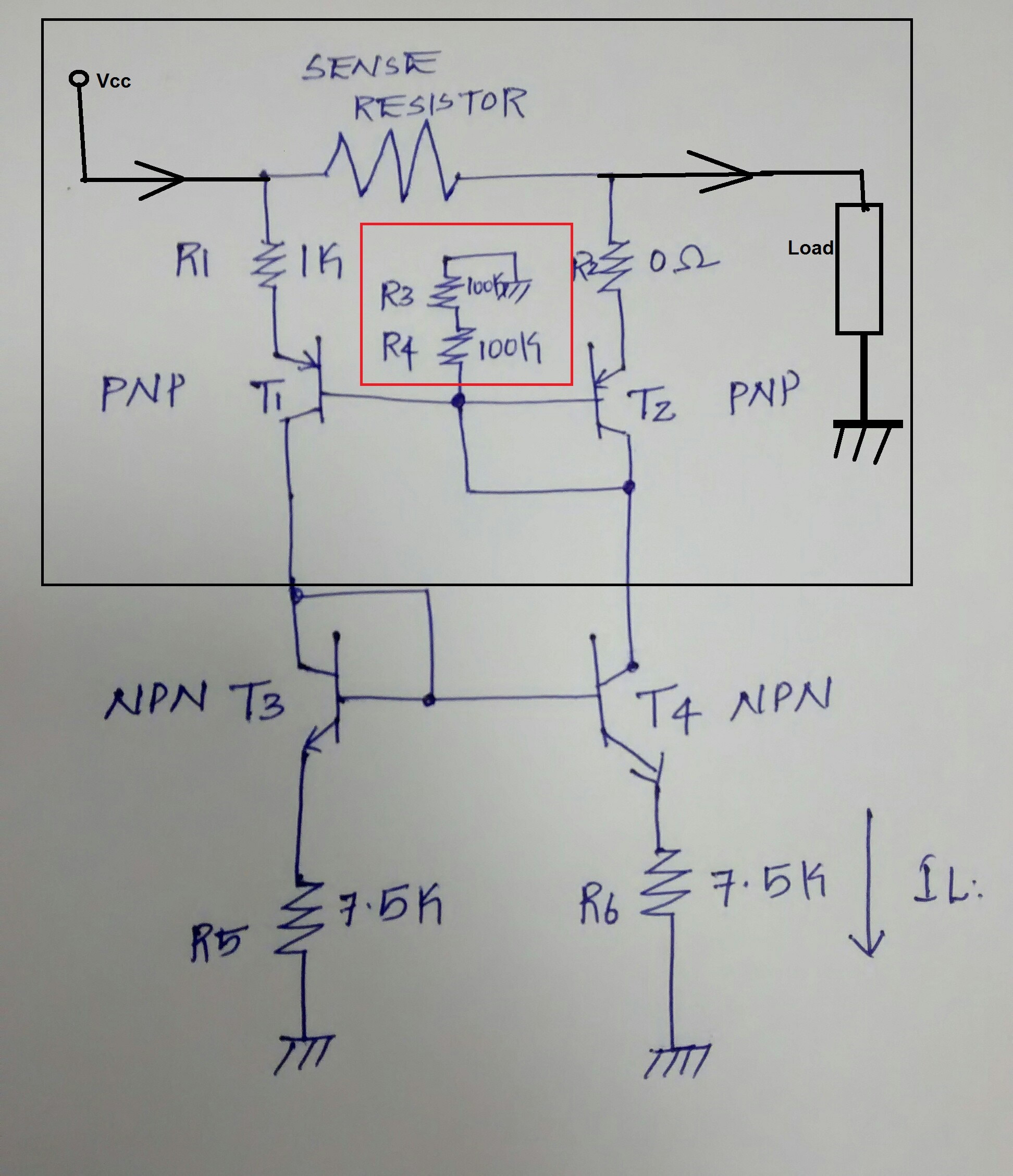
Attached is the circuit I am trying to learn, Lower part with NPN transistors (outside the boxes) are familiar circulatory and and it is self explanatory as well. I am not sure how to is the working of the PNP transistor section (in black box) ?

Also what is the significance of R3 and R4 (red box). How will calculate the value of these resistors.

\$\endgroup\$
4
  • 1
    \$\begingroup\$ This circuit is incomplete, it is not going to work as it does not have a supply connected and it is unclear where it should be connected. \$\endgroup\$ Commented Dec 29, 2016 at 11:59
  • \$\begingroup\$ @FakeMoustache, updated the image \$\endgroup\$
    – vt673
    Commented Dec 29, 2016 at 12:16
  • \$\begingroup\$ R3 and R4 depend entirely what the circuit is trying to achieve and that is unclear from your picture. \$\endgroup\$
    – Andy aka
    Commented Dec 29, 2016 at 12:34
  • \$\begingroup\$ There is a comparator which is connected to the emitter of the T4, output of the comparator is used for the over current protection circuitry. Hope this will clear the ambiguity. \$\endgroup\$
    – vt673
    Commented Dec 29, 2016 at 12:40

2 Answers 2

0
\$\begingroup\$

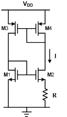
This circuit looks a bit like a reference current generator I sometimes use:
enter image description here

It also works with bipolar transistors so ignore the fact that this circuit uses MOSFETs. Also imagine that R is your sense resistor and the load resistor.

This circuit works by having a 1 : 1 current mirror (M3 and M4) which makes the left and right currents equal. But M1, M2 and R also make a mirror but it is not 1 : 1, it is actually non-linear.

Having these two work together means a solution must satisfy both mirrors.

The wanted solution is where left and right currents are equal but there is also the solution where all currents are zero.

So this circuit needs a start-up circuit to detect that and pull it to the wanted (1:1) solution.

I think that is where your R3 and R4 come in. These force a current through Rsense, R2 and T2 so that the circuit can start up properly.

Once started the current through R3 and R4 will be small, much smaller than the nominal current the circuit is designed to run at. That explains the relatively high value of R3 and R4.

I would have drawn R3 and R4 not up but down from the base of T2 so that it is clear they conduct a current to ground.

\$\endgroup\$
0
\$\begingroup\$

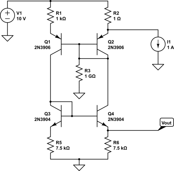
Try simulating the circuit:

schematic

simulate this circuit – Schematic created using CircuitLab

If you run the DC sweep that I have set up, you'll see that the output voltage is a very linear function of the load current.

I'm not sure about the nature of your confusion. The upper current mirror produces a current at the collector of Q1 that is a fraction of the load current. The proportionality is based on the ratio between R1 and R2 (Rsense in your circuit). This current produces a voltage across R5 that is proportional to the load current.

The lower "current mirror" is really just an output buffer; it replicates the voltage across R5 across R6, which isolates it from the effects of any load that you might put on Vout. If you change the value of R6, it produces only a tiny error in the output voltage.

The function of R3 (and R4 in your diagram) seems to be intended to provide some bias current to the upper current mirror (or "start up" current, as FakeMoustache suggests), but all this does is create an offset in the readings at low load currents, adversely affecting the linearity of the circuit overall. Since far more current flows through Q4, they seem to be redundant. Try playing with the value and rerunning the simulation.

\$\endgroup\$

Your Answer

By clicking “Post Your Answer”, you agree to our terms of service and acknowledge you have read our privacy policy.

Not the answer you're looking for? Browse other questions tagged or ask your own question.