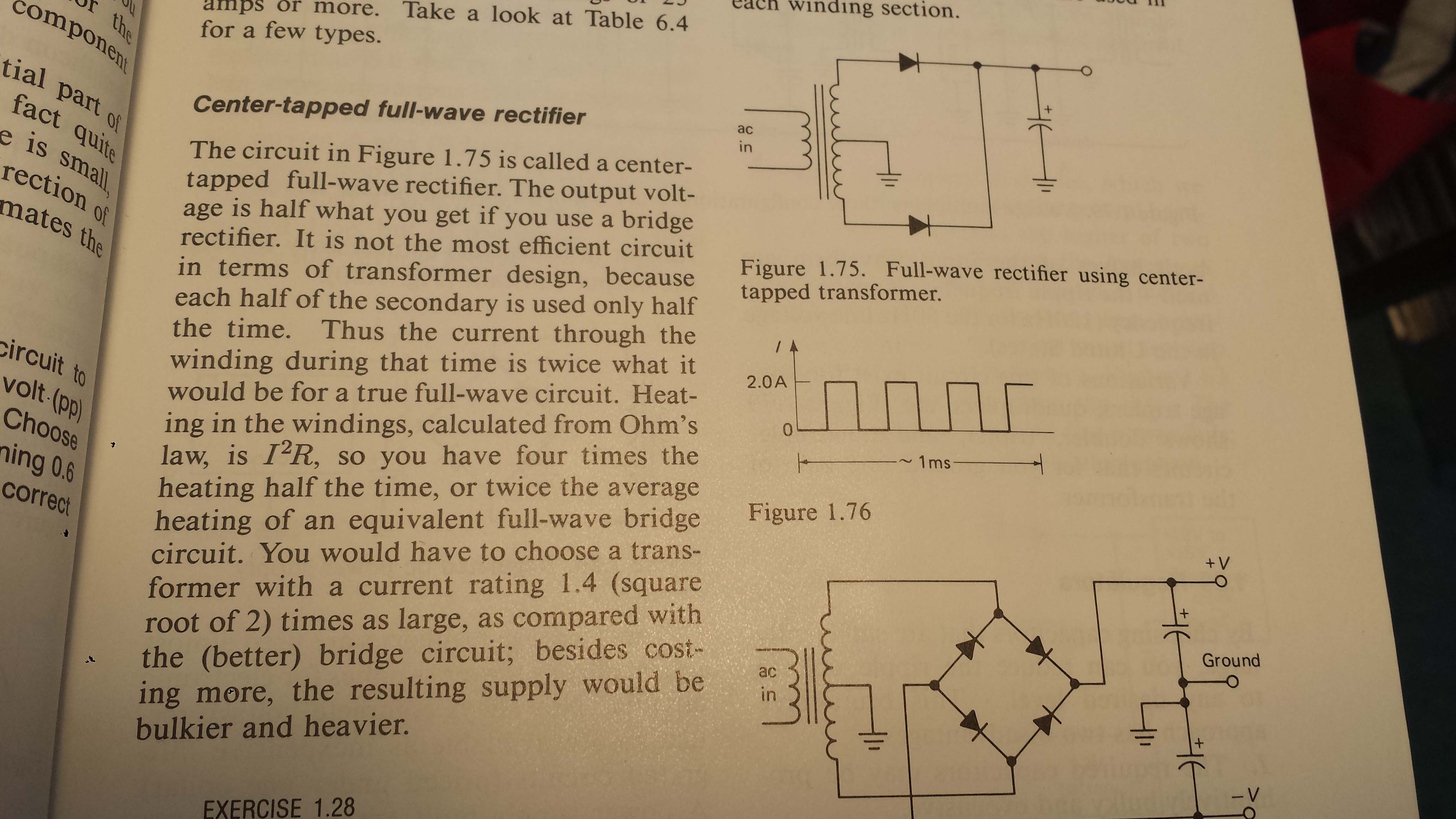
 In the above image, I'm trying to understand the statement that says this is center tapped transformer is less efficient and the current is twice what it would be for a true full-wave circuit. I also have an LPSpice and inductor quesiton later? I did not print the full wave bridge circuit that was on the prior page. In that circuit, it looked like the transformer was 1 to 1 (not step up or down). In figure 1.75, the center tapped transformer looks like it steps the voltage up 2X, except that each half the voltage is 1/2. If this is so, the voltage would be the same as the non stepped up transformer in the full wave bridge circuit that the book might have refered to (and I tried to model below). I was trying to use ltspice to see current and voltage to get a sense of why it is less efficient, but didn't see that?
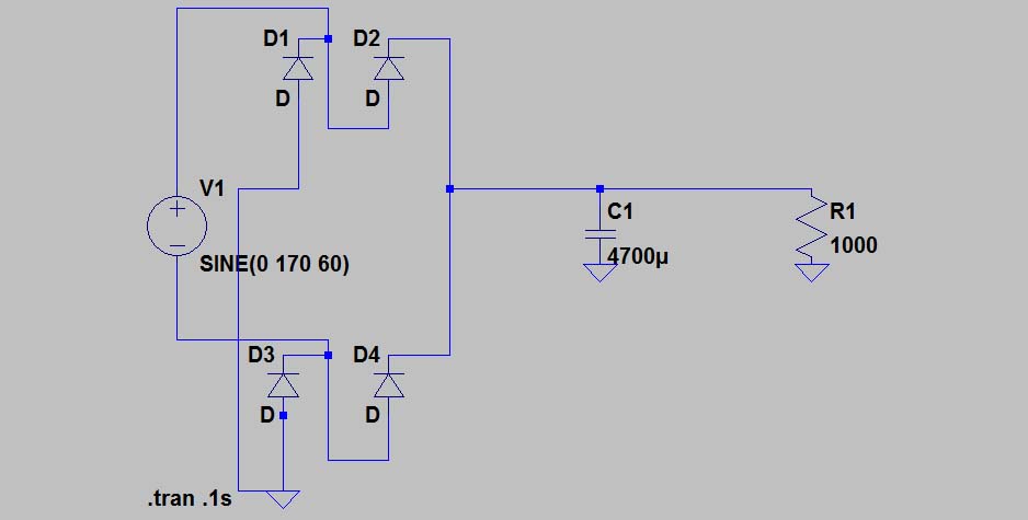
 In this LTspice sim, i did not show the transformer that looks to be 1 - 1 . I spent time testing voltages. When I test the voltage on either side of V1, it does not ever go negative, is this because of the diodes? If so, what happens, when V1 tries to go negative and instead goes positive?
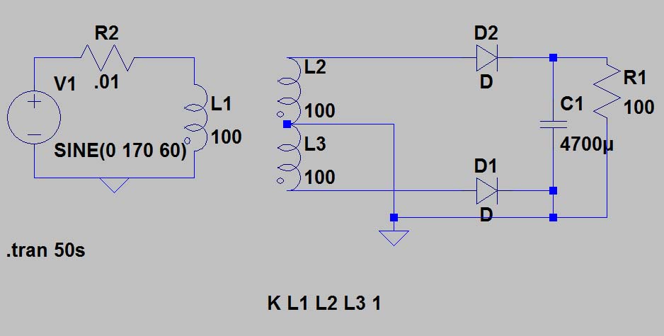
 In this image, VI, tested between R2 and the + sign, oscillates between +160 and -160. When I test between R2 and L1, the negative drops out. I only get values between 0 and +160 through time. Where did the negative part of the wave go? I suspect that its because of the diodes on the right side of the circuit, but don't understand how this "decoupled " side affects the negative waveform on the left side of the image? The above is the center tapped transformer. If the negative part of the input drops off, then I can see how this transformer could be working harder. Any ideas on what happened to the negative partof the wave?
Art Of Electronics - Center Tapped Transformer Efficiency and Current Question, LTSpice Question too
-
1\$\begingroup\$ Why are you so bold? \$\endgroup\$– Andy akaCommented Jan 13, 2017 at 18:07
-
\$\begingroup\$ @Andyaka Unintended, excessive abuse of *, I think. (Perhaps ignorant of what stackexchange does with them.) \$\endgroup\$– jonkCommented Jan 13, 2017 at 18:10
-
\$\begingroup\$ Edit the boldness \$\endgroup\$– winnyCommented Jan 13, 2017 at 18:20
-
\$\begingroup\$ Edited. I thought the text stood out better. I did not know that Stackexchange has special processing/criteria for bolded text. I will review. \$\endgroup\$– Jeffrey Edward MessikianCommented Jan 13, 2017 at 20:46
-
\$\begingroup\$ If you read the text right under the statement of why it's not so efficient (if I might be so bold), it tells you!. I don't see how anybody is going to put it plainer than that! RMS current (heating) is increased, per output current. \$\endgroup\$– Neil_UKCommented Jan 13, 2017 at 22:10
3 Answers

simulate this circuit – Schematic created using CircuitLab
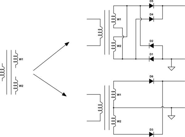
Use a transformer that can be set up to give the same output voltage in either the full wave bridge or center-tapped full wave configurations. It is illustrated above where I drew only the necessary details for showing the differences. It is under this context, which you start with the same equivalent transformer, that the explanation you posted is applicable and makes the most sense.
In the bridge configuration, both windings (W1 and W2) conducts every half cycle and therefore share the output current every half cycle.
In the center-tapped configuration, either W1 or W2 conducts every other half cycle, but never the same time. Therefore only one winding supplies the total output current during a half cycle.
Update responding to comments:
Let's use a solid example. The following is from a datasheet I got from Digikey, it is the first one in the table when I chose power transformer. http://catalog.triadmagnetics.com/Asset/FS12-090-C2.pdf

The two output split windings can be used by connecting them in series -- pin 5 and 8 as output, pin 6 and 7 tied together. Then used in a full-wave center-tapped configuration with pin 6&7 going to ground. The output voltage would be rectified from 6.3Vrms. The current limit would be 0.09A for this comparison.
The two output windings can be used by connecting them in parallel -- pin 5 & 7 together, and pin 6 & 8 together. Then used in a full-wave bridge. The output voltage would also be rectified from 6.3Vrms. When used with a current of 0.09A, the current through each windings is only half of the specification and therefore has half the total conducting loss as comparison (this is the point of the pasted explanations in the OP). Alternatively, the output current limit can be as high as 0.18A all within the transformer specifications.
For the full-wave centered tapped configuration, it is possible to cheat and draw more than 0.09A because the transformer is rated for 1.1VA (approximately 6.3V x 0.18A). But the transformer specifications would no longer be 100% applicable because the 0.09A current limit through a winding in the datasheet would be exceeded and one would need to apply some extrapolations. For example, the 25% typ voltage regulation would probably be exceeded.
So here is the real big disadvantage of the center tapped configuration in this real component example -- you either operate the transformer at half the rated power while staying all within spec, or you can operate the transformer at closer to the rated power with extra power loss and some specifications would be exceeded and required extrapolations.
But the real reason for the center tapped configuration is to rectify both a positive and negative 6.3Vrms rectified voltage from it. With this transformer, the within spec output limits would be 0.09A for positive and 0.09A for negative.
It is also possible to connect the two windings in series -- use pin 5 and 8 as outputs, pin 6 & 7 together and go nowhere. Put a bridge rectifier on pin 5 and 8. Then the output would be rectified from 12.6Vrms and current spec would be 0.09A max.
-
\$\begingroup\$ This is interesting. The bottom image is definitely the center tapped transformer in the book. In the top image, can you explain the transformer a little? I see the transformers are equivalent except for the center tapp, but what are the outputs in the top transformer? The bottom transformer should have only two, which it does, the top should have just one? In the top image, W1 and W2 look parallel, what does that do? I guess that is double the windings? \$\endgroup\$ Commented Jan 13, 2017 at 21:45
-
\$\begingroup\$ Go look up some actual transformer (for DC power supply applications) datasheets, you would probably find that the most common configuration of the transformers is the split output windings like above. For the same equivalent output voltage, you can connect the windings in parallel to get better current characteristic (as explained in the pasted image) but extra diodes and one extra diode voltage drop. Or connect the windings in series for center-tapped for less diodes. \$\endgroup\$– rioraxeCommented Jan 13, 2017 at 22:28
-
\$\begingroup\$ While the one compiling reason to go center-tapped configuration would be if both positive and negative outputs are needed, which your pasted image seems to be getting to. \$\endgroup\$– rioraxeCommented Jan 13, 2017 at 22:29
-
\$\begingroup\$ In the top image, When the input sine wave transitions say from 0-1-0, at this point W1 and W2 conduct and current flows to D4 and D5? Correct? When the sine wave goes from 0 to -1 and back to 0, the voltage is negative, and current is pulled from d1 and d2, if ground sourced current.which it doesn't, hence the, the half cycle. right? \$\endgroup\$ Commented Jan 14, 2017 at 1:54
-
\$\begingroup\$ During the half cycle when the top of the windings is positive, the possible path of current flow is from top of the windings, through D5, through the load, through D1 back to bottom of windings. During the opposite half cycle when the bottom is positive, bottom -> D4 -> load -> D2 -> top. \$\endgroup\$– rioraxeCommented Jan 14, 2017 at 6:07
The text does a great job of explaining things. Try the following in LTSpice:

simulate this circuit – Schematic created using CircuitLab
(No need for inductors for this test.)
How, make sure that \$R_1\$ and \$R_2\$ are exactly the same value. You will want the exact same current flowing through these two resistors so that the exact same driving voltage appears across them. That's your load and you want the same power dissipated in the load in both example cases. So \$R_1=R_2\$.
You will also want the series capacitance exhibited by \$C_2\$ and \$C_3\$ in the right-hand case to be the same as \$C_1\$ in the left-hand case. So this means that whatever you set \$C_1\$ to, double the value for \$C_2\$ and \$C_3\$. This will mean that the net re-charging portion of the cycle will be the same in both cases. You need to make \$C_1\$ large enough that you don't see much variation in the current in \$R_1\$. For \$60\:\textrm{Hz}\$, I'd probably make the RC time constant about 3-4 seconds, just to be safe. So set \$C_1=\frac{4}{R_1}\$ and set \$C_2=C_3=2\cdot C_1\$.
You need to select diodes that are appropriate for the current load. Whatever they are, use the same ones across the board.
Now, set \$V_1=V_2\$ and set \$V_3=V_4=\frac{1}{2}\cdot V_1\$ to start out. This actually won't work perfectly, just yet. But it should get you close. Measure the current in \$R_1\$ after one second's time (.tran, I suppose) and then make small adjustments (probably upward) in the values for \$V_3\$ and \$V_4\$ (keeping both always the same) until the current in \$R_2\$ is the same as the current in \$R_1\$.
Once you've done that much, you have the exact same load in both circuits and you can now see the differences.
Check out the current pulses coming from all four voltage sources and the timing of them. Look at the peak values and compare them. Do you find them somewhat close to what is talked about in the text?
-
\$\begingroup\$ I have to wrap my head around what you said a little. It seems quite different than the text, even as an explaination to my question. For instance, in your Fullwave bridge, you have two capacitors, the text has only one, when it was describled on a page earlier. Both exhibits in the text were shown with transformers. The reason for the inductors in my exhibit is that LT spice does not have transformers. I read how that can be simulated with inductors that are linked. In any case, both of my circuits seem to produce DC output that has a small ripple. \$\endgroup\$ Commented Jan 13, 2017 at 21:25
-
\$\begingroup\$ I understand everything in the text except for only one line.... The line I'm trying to get my head around is "the center tapped transformer is less efficient and the current is twice what it would be for a true full-wave circuit." Why is the current doubled when each half appears 1-1? Only whats in quotes is what prompted me to write this question. \$\endgroup\$ Commented Jan 13, 2017 at 21:25
-
\$\begingroup\$ @JeffreyEdwardMessikian Regarding the two capacitors, feel free to replace them with just one and no ground center tap. I did that to just tie in a ground-center there. It's not important. If you replace them both, then use the same value, instead of twice the value I'd earlier indicated. \$\endgroup\$– jonkCommented Jan 13, 2017 at 22:20
-
\$\begingroup\$ @JeffreyEdwardMessikian Regarding your last question, I was trying to set you up with a situation where you can see the difference with LTSpice. You will see lower current peaks in the voltage sources on the right-hand side, even though the load is receiving the same voltage (and of course current.) When you see that fact, then also notice how often those peaks occur one vs the other. That may help you "see" why. \$\endgroup\$– jonkCommented Jan 13, 2017 at 22:22
Where did the negative part of the wave go?
Your final circuit is wrong - the two cathodes should join i.e. D1 cathode should go to the top of the capacitor. At the moment you are shorting out the transformer on half cycles.
-
\$\begingroup\$ I edited the circuit to match figure 1.75. I did notice that D1 was put in wrong. The output looks pretty close to DC with a small ripple. I can play with things later. But, I think that this works ok in LTSpice. \$\endgroup\$ Commented Jan 13, 2017 at 21:11
-
\$\begingroup\$ It was the top circuit that seemed to drop the negative cycle somewhere. First, let me say.. the top circuit also works in LTSPice .The output is pretty close to the other one. In fact, the top circuit has less ripple. When I connect the LTSpice volt meter to either the positive or negative lead of V1, in the full wave bridge (with D1-D4) there are no negative cycles. It appears that the positive cycle is shifted 180 out of phase on either terminal. I was just wondering where this went? Though, the output does look like DC and I suppose if it was built, it wouldn't go boom. \$\endgroup\$ Commented Jan 13, 2017 at 21:12
