1
\$\begingroup\$

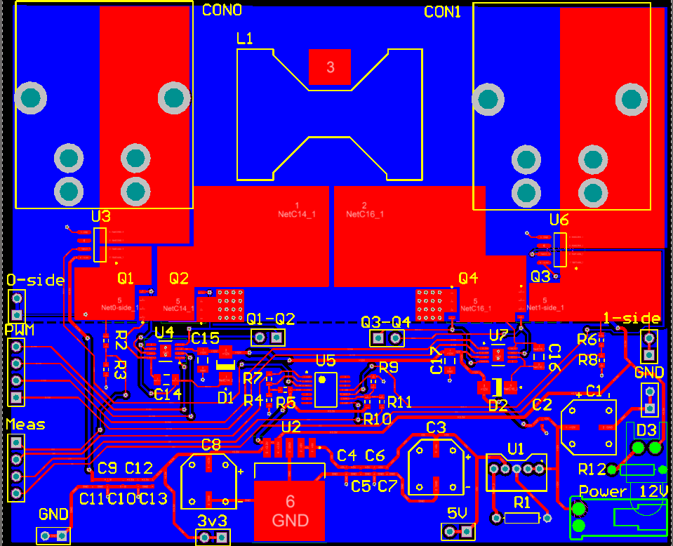
I am designing a bi-directional DC-DC converter for automotive use. Therefore, there is some high-power stuff that needs to be implemented on the pcb. The overal layout is as such:

PCB Layout

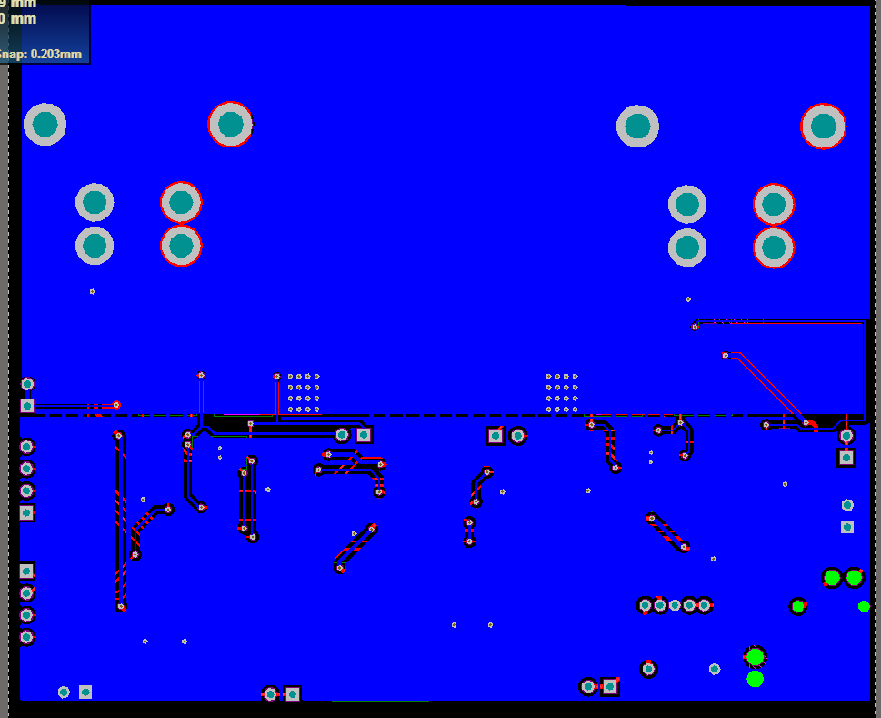
My question is if I should separate the high-power and low-power ground-planes? If so, how would I do this? They do need to be connected somewhere, so I'm not sure where I would do that? For now I have it like this:

PCB Layout ground-planes

So there are two 'big' ground-planes, and attached to each other in the center through smaller tracks. Do I remove the tracks and connect somewhere else entirely, or would this work?

Furthermore, I would greatly appreciate some general advice on my design as this is my first PCB, and I am still pretty inexperienced. The reason for all the pins is because this is supposed to function as a test board.

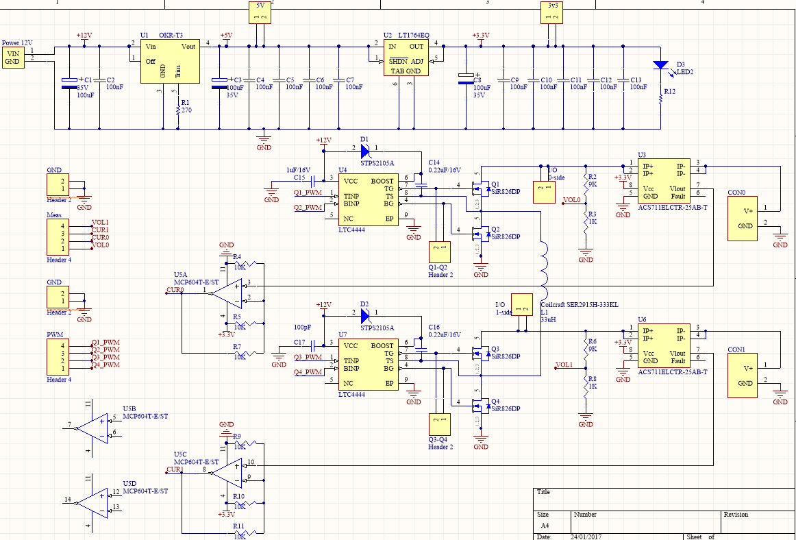
Here's the schematic:

enter image description here

\$\endgroup\$
8
  • 1
    \$\begingroup\$ Feedback on test pins: you can generally not have too much of them. In fact, I see test pins especially on boards designed by experienced engineers, and unless you're talking about very high integration, even in production PCBs – you'll never figure out why 1% of your boards fail in the field and be able to take your PCB manufacturer into regression for that if you don't find that voltage that isn't as clean in the production PCB as it was in the prototype PCB if you don't have test pins. \$\endgroup\$ Commented Jan 24, 2017 at 15:41
  • \$\begingroup\$ Just be a bit careful with routing fast signals: a stub line does modify the signal on a trace by acting as a reactive component at sufficiently high frequencies. \$\endgroup\$ Commented Jan 24, 2017 at 15:42
  • \$\begingroup\$ The PWM pins are actually not stub lines. The pins are the actual input of the PWM from an external micro. PWM is around 100kHz. Would the length of the traces interfere with/modify the signal? \$\endgroup\$ Commented Jan 24, 2017 at 15:48
  • \$\begingroup\$ modify: yes. That being measurable: I don't know – depends on the receiving part, I guess, but at 100 kHz, I wouldn't worry too much :) \$\endgroup\$ Commented Jan 24, 2017 at 15:53
  • 1
    \$\begingroup\$ Just looking at the PCB is kind of useless without a schematic, I can infer what most of the parts do, but as to the overall function of the board I have no clue. In the least you should give a list of the function of the important parts. Where is your power input? Is it 12V or one of the CONS? \$\endgroup\$
    – Voltage Spike
    Commented Jan 24, 2017 at 17:20

3 Answers 3

4
\$\begingroup\$

This board will not work...

There are no capacitors on the input and output of your DC-DC !

Come on... Considering the huge size of the inductor, and the fact there are ACS711-25, it's at least 10 amps... Please, please, please. Stick a healthy amount of ceramics, plus some low-ESR bulk caps both at the input and at the output.

Consider this:

  • Q3 OFF, Q4 ON, I(L)=5A
  • Q3 turns on, Q4 turns OFF
  • Inductor current must now go somewhere (in the output)
  • However, there are no caps. This means the current must go into the inductance of the wires...
  • L1 will generate enough voltage at the output to force its current wherever it has to go.
  • All components at the output will blow.

Now, layout. I'll start with the MOSFET drivers.

You want the current loops to be small to ensure fast and clean switching, without ringing. For U4 driver and Q1/Q2 FETs, loops are:

  • Q2 turn-on: GND-C15-U4.VCC-U4.BG-Q2.G-GND
  • Q2 turn-off: GND-U4.GND-U4.BG--Q2.G-GND
  • Q1 turn-on: U4.TS-C14-U4.Boost-U4.TG-Q1.G-Q1.S-U4.TS
  • Q1 turn-off: U4.TS-U4.TG-Q1.G-Q1.S-U4.TS

Also C14 charging loop should be optimized:

  • GND-C15-D1-C14-Q2-GND

Layout error: these loops are quite long, and they run over splits in the ground plane. Gate drivers are not sensitive analog opamps! You can locate them close to the FETs, with short traces for gate drive... and optimize decoupling caps placement! (I see a split in GND plane between your decoupling caps GND and the chip's GND)...

----------------------- EDIT

Your Hall current sensor is isolated, which means you should reference its output to signal ground, not noisy power ground. Also check if it needs a decoupling cap.

Also, its output is centered on VCC/2, which is your 3V3. If this 3V3 is different from the one used in the micro, you will have DC offset.

MCP604 does not have rail to rail input, which might be incompatible with ACS711 output voltage.

Did you check the MOSFET thermal dissipation?

80V FETs seem a bit high for automotive use. Perhaps you could get better RdsON*Qg with 40-60V FETs?

Can't find datasheet for STPS2105 diode.

Look at C9-10-11-12-13, why are your decoupling caps clumped together in a corner of the board, instead of close to the chips they're supposed to decouple?

Schematic says U2=LT1764EQ, which is not the 3V3 part. Also, do you need big expensive LT LDO here?

Placement of GND vias for capacitors C3, C8 is... uhhhh... are there even any GND vias?

But... This kind of DC-DC is DIFFICULT to pull off. This is really really NOT the kind of circuit you want to do for your first PCB! There are so many mistakes here... and every time I look at it I find more... and it's normal since this is your first PCB, as you say.

There is no way a beginner will succeed on this kind of design. I'm not trying to bash you or insult you, OK? But you risk burning tons of parts, wasting a week in frustration, and it will probably not work.

There is also the fact that this is PWM-controlled, so a software bug can make your FETs explode. And you didn't choose the easiest package to desolder...

I strongly suggest you seek help from someone qualified who can look over your shoulder and help you, this will avoid lots of butthurt.

\$\endgroup\$
1
  • \$\begingroup\$ What is the voltage of automotive load-dump? when the alternator suddenly has NO BATTERY to provide a load? 80 volts? \$\endgroup\$ Commented Apr 6, 2019 at 8:19
1
\$\begingroup\$

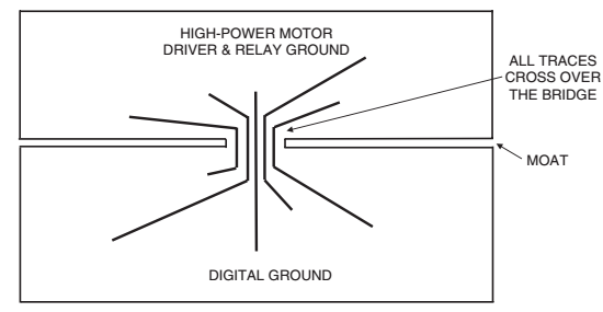
The cuts you have created in your ground plane does not have any effect on the separation you have in mind. This is referred to as a 2nd basic problem in mixed-signal circuits when low frequency high current circuits such as switching MOSFETs or relays are in your PCB and they interfere with low-level analog and digital circuits. You need to create a moat or completely isolated ground.

This is one possible solution

\$\endgroup\$
0
\$\begingroup\$

Please compute some of the magnetically induced voltages, particularly from high-fast-current loops, into the servo-regulator circuits. A combination of Biot_Savart and Faraday Law Induction gives you the ability to compute the voltage induced in loop, given a dI/dT & dB/dT of nearby wire.

Vinduce = [MUo*MUr * Area/(2*pi*Distance)] * dI/dT

Assume dI/dT is 10 amps in 10 nanoSec, (very fast FET switch) in aggressor wire.

Assume vulnerable loop area is 0.1meter * 0.1meter, located 0.1meter from wire.

Vinduce is 4*pi*10^-7H/m *1(air)*0.1m*0.1m/(2*pi*0.1m) * 10^+9 amps/second

Vinduce is 2e-7 * 0.1 * 1e+9 = 2e-8+9 === 20 volts.

In such magnetic fields, particularly very fast edges, the servo-system is trashed.

Think about shielding the regulator feedback servo circuits.

By the way, this Hfield (magnetic field) interferer is built into the GARGOYLE function of SignalChainExplorer, available at robustcircuitdesign.com

The intention is to aid the embedded system designer, to model all relevant error sources, avoiding the surprises of phenomena often ignored.

---------------- edit ----------

At previous job, the Customer Rep invited me into a phone call, where the Customer had a lines-down problem with our silicon, which they had used successfully for a decade. Something had changed, and their 15,000 Horsepower motor speed controller was failing in the field. At various locations on the Controller PCB, various of our silicon failed. But not at all locations.

Some locations never have failures. Other locations had 25% of the failures. Yet the PCB has 6 layers with lots of heat removal paths. What was going on?

We compute Vinduce = 2e-7 * 40mm * 40mm/40mm * 2e9 amp/second

The Control PCB was 40mm away from 2,000 amp bus, switching on/off in 1uS.

Vinduce = 2e-7 * 0.04 * 2e9 = 0.16 * 100 = SIXTEEN VOLTS

There was 16 volts induced into the GROUND PLANE. Call it an eddy current. Certainly some Hfield cancellation occurred.

Customer complaint: your parts fail. Our response: you've moved the PCB way too close to the 2,000 Amp bus. Customer: help us. Our response: place aluminum shield between PCB and Bus.

SUMMARY: WHEN YOUR SWITCHING CIRCUIT exceeds 100,000,000 amps/second dI/dT, you must expect huge upsets to Grounds, Ground planes, to VDD, to VDD planes, to feedback regulation pins, and indeed to any trace.

\$\endgroup\$
0

Your Answer

By clicking “Post Your Answer”, you agree to our terms of service and acknowledge you have read our privacy policy.

Not the answer you're looking for? Browse other questions tagged or ask your own question.