0
\$\begingroup\$

I'm using MP2359 for converting 12V from 20V.

Datasheet: http://www.monolithicpower.com/desktopmodules/documentmanage/api/document/getdocument?id=269

I'm using the recommended sch and layout designs (SCH on the first page).

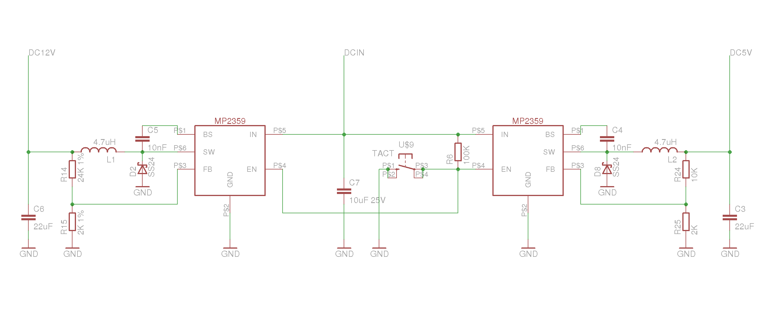
My resistors are 2K and 24K to have 12V, and I use the recommended Wurth inductance just for being sure about everything. My Schottky is SS24, which is basically the same as the recommended one (it's not available in my place).

Now P#4 (Enable) is connected to P#5 (In) thorugh a 100K resistor to enable immediately as there is voltage on the input side, and I have a tact switch also on P#4 which connects it to GND when I press it. (Reset button)

Currently there is no load on the output, just a 22uF capacitor. (will drive relays later)

If I turn on the input power, it creates 12V nice and smoothly.

However, if I press the reset button, and release, the chip dies, and shorts P#5 and P#6 (input and output), resulting high voltage on the output.

I'd love to hear something useful of the root cause of this. Burnt 6 pieces just today while trying to analyse what is happening.

What I have tried?

  • I was constantly monitoring the output at the capacitor.
  • If I turn down the input, after a few seconds voltage collapse to 0.
  • Turning it back again output goes up to 12V.
  • Repeated this a few times (but always waited for the 0 voltage after turning off) -> always succeeded.
  • Then push the reset button (Enable pull down to GND), wait for 0V @output.
  • Upon releasing the reset button, output goes above 12V until it reach the input voltage.

EDIT

SCH: http://94.21.0.105/dcdc.png

DC5V has a load of a microcontroller. DC12V has currently no load on it (it is connected to a SI2307 P-MOSFET's source)

After pressing the TACT, MP2359 on the left dies, but MP2359 on the right doesn't.

\$\endgroup\$
5
  • \$\begingroup\$ Are you saying that p4 is shorted to p5 and not through a resistor? In this case, your reset button is shorting out your input. Not saying that this could cause the observed problem, just noting another problem or you're not being caseful im describing your setup. \$\endgroup\$
    – DoxyLover
    Commented Jan 29, 2017 at 21:58
  • \$\begingroup\$ Of course P#4 is connected to P#5 through a 100K resistor. Sorry. \$\endgroup\$
    – Daniel
    Commented Jan 29, 2017 at 22:32
  • \$\begingroup\$ Add schematic!! \$\endgroup\$
    – winny
    Commented Jan 30, 2017 at 13:13
  • 1
    \$\begingroup\$ Could very well be layout. Is this on a PCB or is this breadboarded? Did you verify the pin 4-5 short after removing DCIN and allowing everything to discharge? Why do you only have a single 10uF cap on DCIN (each switcher needs one and it needs to be as close as possible to the IN and GND pins). You could also put a small capacitor from the reset pin to GND to provide a slower-rise enable signal and mask some of the switch bounce. \$\endgroup\$ Commented Jan 30, 2017 at 14:13
  • \$\begingroup\$ Pin4-5 is shorted for sure, it's measurable even after desoldering it from the board. Single 10uF could have been a good point, but in this case DCIN is coming from a stable 20V PSU (SMPS) which has its own large buffer cap. Anyway 10uF can't be any closer to the 12V MP2359. I'll try the reset small cap though. \$\endgroup\$
    – Daniel
    Commented Jan 30, 2017 at 16:35

2 Answers 2

1
\$\begingroup\$

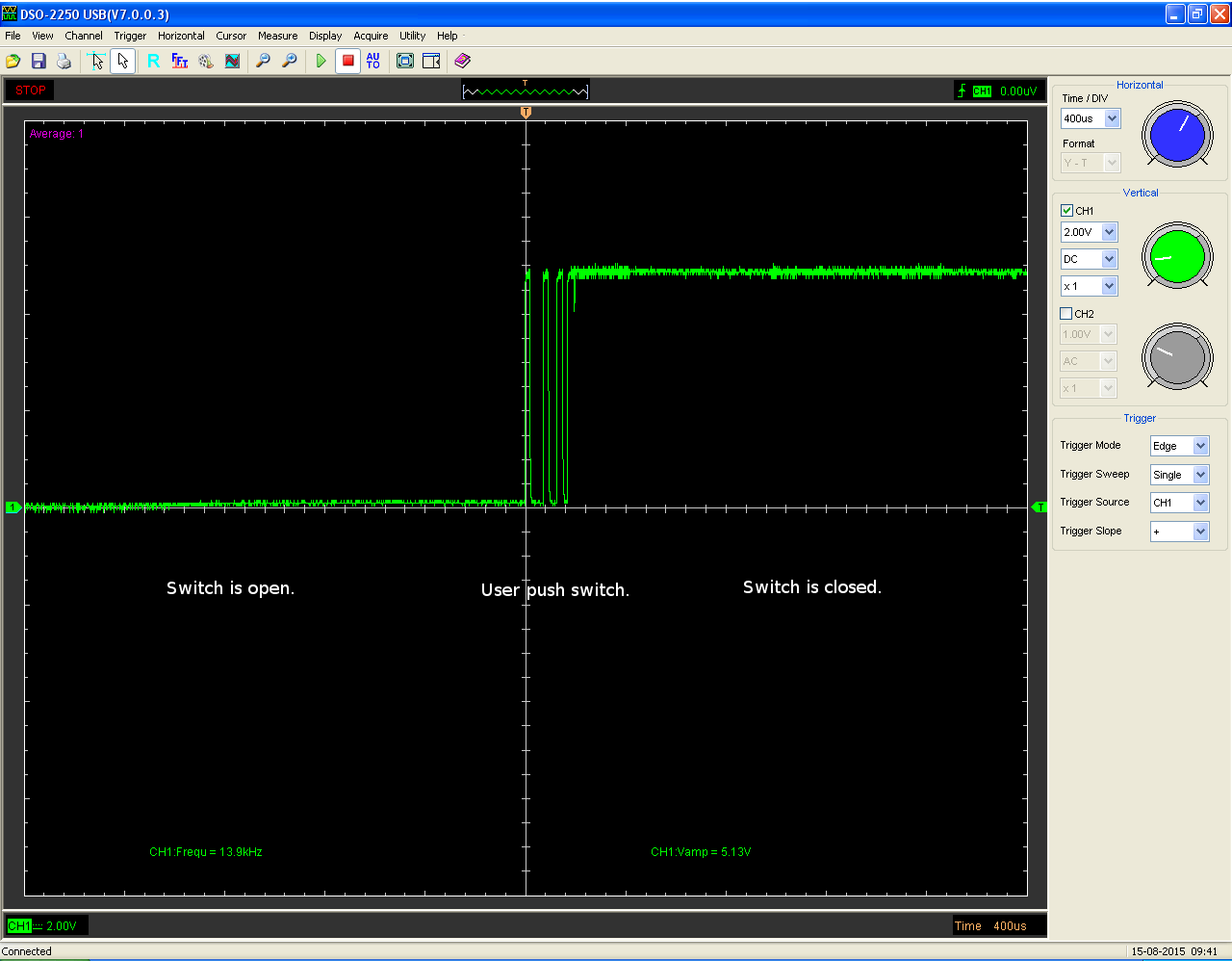
I think you have a problem with switch bounce. EN is probably not designed to deal with the erratic bounce from a switch; it was probably designed to be driven by a CPU or other logic.

Instead of repeating info here, take a look at the excellent debounce tutorial at allaboutcircuits.com The plot below is from that site and is probably what your EN signal looks like.

enter image description here

The reason that turning the input on and off does not cause problems is because a well designed SMPS IC is designed for this and gracefully resets itself when the input voltage drops too low (see "undervoltage lockout" spec).

I suspect that it gets damaged only when EN goes high because at startup the SMPS is under very heavy load as it charges up the 22 uF output capacitor. If your switch glitches then, the switching logic may be getting corrupted and leaving the internal pass MOSFET on too long causing the inductor to saturate. When that happens, the inductor current skyrockets and the pass MOSFET is damaged from overcurrent.

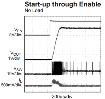
You can confirm this hypothesis by replicating the "Start-up through enable" plot shown in the datasheet. Monitor EN, SW and VOUT with the sweep set at 200 us/div and trigger on the rising edge of EN just like they show. IL would be handy if you had a DC current probe. From the datasheet, here's what it should look like.

Start-up plot from datasheet

If this hypothesis is correct, then you should see switch bounce as EN goes high and then SW will get stuck at 12V right at the point when the pass MOSFET gets damaged.

\$\endgroup\$
3
  • \$\begingroup\$ Nice description. Now I have another MP2359 on the same input, which produces 5V. On that 5V there is a load, and it can survive the 'reset'. The two MP2359 P#4 is common, and so their P#5 too. Is this aligned with your hypotesis? \$\endgroup\$
    – Daniel
    Commented Jan 30, 2017 at 7:10
  • 1
    \$\begingroup\$ Nope. That does not align with the hypothesis. However, something like this (glitching on the EN input) may not be operating in what the IC design engineer had expected and something product/test would not have tested for so it could be some unexpected side effect that happens at lower output voltages or with no load. It is hard to say. But taking the scope plot and sacrificing a few more parts would go a long way in proving it out. Also, you should definitely contact an FAE at Monolithic Power to see if they can help you out or have some insight. \$\endgroup\$ Commented Jan 30, 2017 at 15:33
  • \$\begingroup\$ Symptoms were misleading, it was not just afte the button, but sometimes (rarely) even after powerup. Thanks by the way. \$\endgroup\$
    – Daniel
    Commented Feb 1, 2017 at 9:09
1
\$\begingroup\$

Problem was the Schottky-diode. It was simply too far from the MP2359.

MP2359 has a MOSFET inside which handles the switching. This transistor burned out everytime after pushing the reset switch if there was no load on the output.

Now, if there is no load, there is simply no reason for a transistor to die. There had to be a huge current coming from somewhere to kill it.

Without load, the only place where current can flow back to the MP2359's MOSFET is the inductor, which is normally protected by a Schottky-diode.

The inductor was a bit too far from the IC (8mm) and until now I thought that protecting Schottky needs to be as close as possible to the inductor itself. After putting this diode right next to the MP2359 instead of the inductor, the problem completely went away.

So, to draw the lesson: protector Schottky has to be as close as possible to the protected part, and not to other components which it is protecting the part from.

\$\endgroup\$
2
  • 1
    \$\begingroup\$ I think it's most critical to put the GND of the Schottky diode and output cap C2 right at each other. When the internal MOSFET shuts off, the end of the inductor at the SW net swings below GND and this diode gets forward biased and conducts current through C2. It's this loop that has to be very low impedance otherwise the SW pin has negative spikes which can damage the internal MOSFET. The datasheet has a good example layout which should be followed. \$\endgroup\$ Commented Feb 1, 2017 at 19:10
  • \$\begingroup\$ This could be right, but currently C2 and the Schottky are right next to each other. Distance between them is less than 1mm. \$\endgroup\$
    – Daniel
    Commented Feb 22, 2017 at 21:13

Your Answer

By clicking “Post Your Answer”, you agree to our terms of service and acknowledge you have read our privacy policy.

Not the answer you're looking for? Browse other questions tagged or ask your own question.