7
\$\begingroup\$

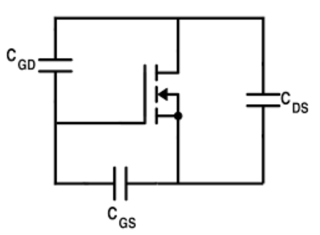
A FET has parasitic capacitance, which can be modeled as a capacitor between each of its terminals (gate, drain and source), which I refer to as Cgd, Cgs and Cds, as shown in the image below.

enter image description here

FET manufacturers list other capacitances in their datasheets, which are refered to as input capacitance Ciss, output capacitance Coss and reverse transfer (or Miller) capacitance Crss. As far as I know, these capacitances are measured as follows:

  • Ciss is measured by shorting drain and source, so it really is the parallel capacitances Cgd and Cgs, hence: Ciss = Cgd + Cgs

  • Coss is measured by shorting gate and source, thus it is Coss = Cgd + Cds

  • Crss is measured between gate and drain (without shorting anything), therefore it is Cgd plus the series capacitance of Cgs and Cds: Crss = Cgd + 1 / (1/Cgs + 1/Cds)

However, when I take a look at the datasheet of an AO3162, there is something strange: this device has typical values of Ciss = 4.2 pF, Coss = 0.45 pF and Crss = 0.05 pF.

Cgd must be very small, so I approximate Cgs = Ciss and Cds = Coss. However, the series capacitance of these is 0.41 pF, much larger than the measured value for Crss. How is this possible?

\$\endgroup\$
1
  • 2
    \$\begingroup\$ What a very useful Fet +1 ,It is as good as a valve. \$\endgroup\$
    – Autistic
    Commented Feb 9, 2017 at 11:58

2 Answers 2

6
\$\begingroup\$

\$C_{rss}\$ is not measured by putting a capacitance meter between gate and drain, and leaving the source open.

It is inferred from the ramping behaviour, which is largely controlled by the Miller capacitance, the gate current needed to charge up the \$C_{rss}\$ capacitor, when the drain is slewing in voltage.

This is equivalent to making a three-terminal capacitance measurement across gate and drain, with a guard terminal on the source. This is capable of measuring all three capacitors in that diagram independently, even for the very different values that are shown.

\$\endgroup\$
2
  • 1
    \$\begingroup\$ Indeed, note the text "DYNAMIC PARAMETERS" above the table listing Crss and also the conditions: "VGS=0V, VDS=25V". Where VDS = 25V makes for a broad drain depletion layer resulting in a small capacitance to the gate. Cgd can vary a lot depending on how the NMOS is used (biasing conditions). \$\endgroup\$ Commented Feb 9, 2017 at 9:07
  • \$\begingroup\$ Ok, I understand. Is it then even possible to calculate the individual values Cgd, Cgs and Cds from the given Ciss, Coss and Crss? If it is not, how do I then model these capacitances to analyse a circuit? \$\endgroup\$
    – kassiopeia
    Commented Feb 9, 2017 at 9:28
5
\$\begingroup\$

Part of the answer can be inferred from Rds(on) which is 500 ohms (max), ten thousand times the Rds(on) of a typical switching MOSFET (say, 0.05 ohms).

High power switching MOSFETs are generally implemented as thousands of smaller MOSFETs connected in parallel, which makes them amenable to VLSI manufacturing processes, but tweaked for higher voltage.

The individual ON resistances of each FET sum in parallel to make the absurdly small values (milliohms) you see for the whole device.

Unfortunately the parasitic capacitance values also sum in parallel, which is why the pF values you'd expect for an individual MOSFET grow to the nF values you see for the total device.

So. if we also scale the Crss by 10000, we would see 500pf(typ) or 700pf(max) which is closer to the values you'd expect for a scaled 50mohm device.

Hence my hypothesis is that this device is a single FET or a small array (2,4 or so) optimised for low current switching where a few hundred ohms Rds(on) don't matter. Die photos would be interesting...

However it's not a full explanation, as the (scaled by 10000) Crss isn't quite in the typical nF range.

But notice the breakdown voltage is unusually high, at 700V? That implies unusually thick dielectric layers, to keep the field strength (in volts/metre) between drain and everything else down to normal limits.

And increasing the dielectric thickness in any capacitor will reduce capacitance.

Between these effects (scaling, and tuning for high voltage) I think we can explain the unusually low capacitance.

\$\endgroup\$
8
  • \$\begingroup\$ I get your point. So actually, when I am searching for a MOSFET with exceptionally low Crss, then it is a good idea to look for a device with high Rds(on) and high breakdown voltage? \$\endgroup\$
    – kassiopeia
    Commented Feb 9, 2017 at 13:11
  • 1
    \$\begingroup\$ I think you'll find a good correlation there. Another approach would be to multiply Rds(on) by Crss for a few FETs to get a figure of merit : see how that correlates to Vds(max). You may find a device family that breaks the curve ... but I doubt it'll break it by much. Now what is your purpose in looking for small Crss? There may be architectural answers, like tetrode valves (or "dual-gate MOSFETs" seen in 1980s RF amplifiers) or cascode configurations, or even ways to cancel Miller capacitance (like 1920s "neutrodyne" circuits) \$\endgroup\$
    – user16324
    Commented Feb 9, 2017 at 13:19
  • \$\begingroup\$ I am following Philipp Hobbs' guide in building a photodiode front end. The circuit's bandwidth and SNR can be substantially improved by inserting a common-base transistor before the transimpedance amplifier, which isolates the photodiode's capacitance from the amplifier's input. However, the whole purpose gets lost if the transistor adds more capacitance to ground (via Cgd) to the inverting input than it used to isolate... \$\endgroup\$
    – kassiopeia
    Commented Feb 9, 2017 at 13:27
  • \$\begingroup\$ OK if you're working into an inverting input there's no Miller multiplication of the reverse capacitance, so a cascode won't give anything from the bandwidth point. \$\endgroup\$
    – user16324
    Commented Feb 9, 2017 at 14:07
  • \$\begingroup\$ Take a look at antena.fe.uni-lj.si/literatura/VajeVT/Tetroda/pdf/BF981.pdf \$\endgroup\$
    – user16324
    Commented Feb 9, 2017 at 14:17

Your Answer

By clicking “Post Your Answer”, you agree to our terms of service and acknowledge you have read our privacy policy.

Not the answer you're looking for? Browse other questions tagged or ask your own question.