1
\$\begingroup\$

I am working on the second stage of an operational amplifier which involves a BJT differential amplifier.

I am trying to increase its bandwidth (part of the requirements. The TA told me that a simple cascode should increase the bandwidth.

I am running simulations and, it seems to me that the cascoded version actually decreases the BW. I have tried to change the biasing voltage with no success and cannot find any source about cascoding increasing the bandwidth.

enter image description here

\$\endgroup\$
1

3 Answers 3

1
\$\begingroup\$

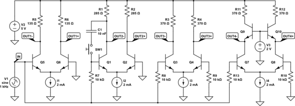
Examine the circuits below. Each of the three differential pairs on the left have differential gain of 4X at low frequencies. Yet their F3dB (45 degree point) are not the same: why?

schematic

simulate this circuit – Schematic created using CircuitLab

And Q7/Q8 - same topology as what you propose - does not have a gain of 8x. It in fact has gain < 1x. Why?

The input and output voltage waveforms for each amplifier circuit

The frequency amplitude response of the 4 circuits The frequency phase response of the 4 circuits

Also notice the leftmost diffpair has no source resistor, thus CMiller can be infinite but the SPICE source handles the input current (Ibase, Cob) just fine; on the other hand, the 3 right circuits include Rin, and that R along with Cmiller impacts the circuit bandwidth.

\$\endgroup\$
0
\$\begingroup\$

Some help: see the cascode circuit at (https://www.allaboutcircuits.com/textbook/semiconductors/chpt-4/cascode-amplifier/) and then work on getting the DC bias of your circuit correct. The CASCODE outputs are at the collector node of Q3 and Q4. Because you have VCC=+15Vdc and VEE= -15Vdc, then when "your circuit is DC biased to operate at QUIESENT current, the DC voltage at Q4collector has to be ~0.0Vdc, so that the AC output of the amplifier can "swing symmetrically" above and below 0 volts. To operate linearly, you have to provide DC bias to get Q4Vce=2V and Q2Vce=2V. This will cause Q1 emitter to be ~ -4Vdc and Q1 base ~ -3V To apply an AC input at Q1base and Q2base, you will need a coupling cap , so that the applied input referenced to 0Volts does not clash with the (-3Vdc) bias at the base of Q1 and Q2. Dont hesitate to use a few resistors to adjust your DC bias, instead of using a SOURCE

\$\endgroup\$
-4
\$\begingroup\$

C = B * log2((S + N)\N)

C = Channel Capacity

S = Signal Power

B = Bandwith

N = Noise power

This means if you want to increase the bandwith without reducing the Channel Capacity(losing the amount of information the circuit can process every second) That you can either increase the Signal Power or decrease the Noise.

\$\endgroup\$

Your Answer

By clicking “Post Your Answer”, you agree to our terms of service and acknowledge you have read our privacy policy.

Not the answer you're looking for? Browse other questions tagged or ask your own question.