2
\$\begingroup\$

I want to make a simple battery powered Arduino-based keypad lock, and in order to save as much power as possible, I want it to self-shutdown after few seconds of inactivity.

I am trying to devise this shutdown mechanism and this is what I suppose should work:

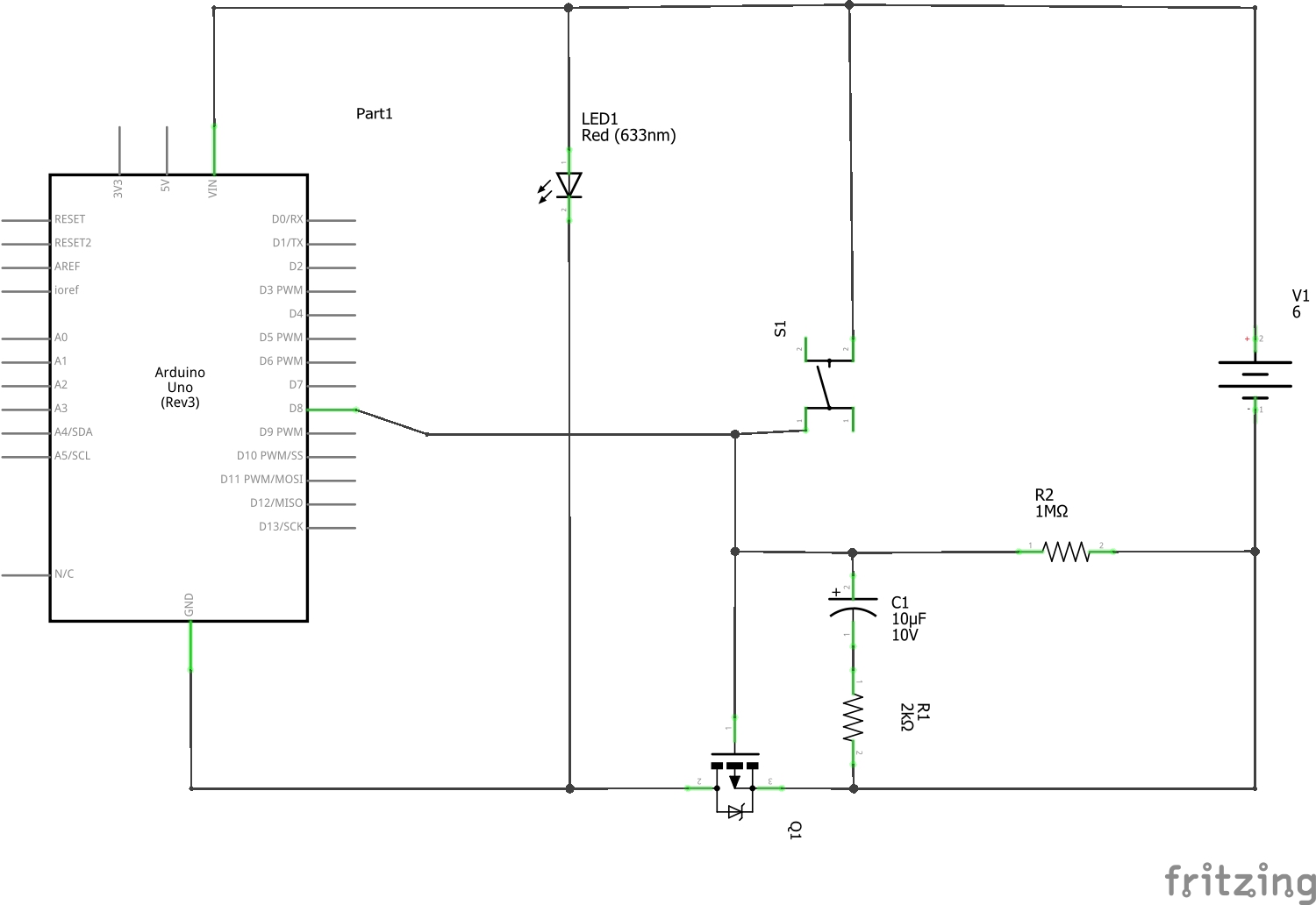
enter image description here

It should work like this: after I tap the switch, MOSFET should start conducting, powering the Arduino and also C1 should charge quickly. C1 should keep MOSFET on for few seconds, allowing Arduino program to load and set D8 pin to logical 1, and therefore to take over business of keeping MOSFET on at all times. After Arduino detects few seconds of inactivity, D8 pin turns off and after C1 discharges, MOSFET turns off, so the whole thing turns off.

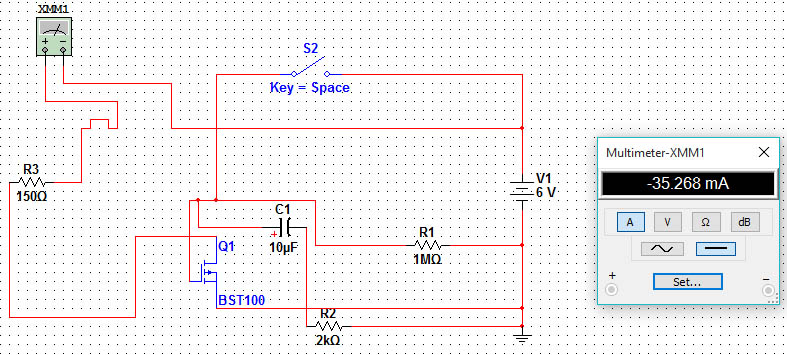
I've entered similar scheme in Multisim software, replacing Arduino with 150 ohm load resistor and ignoring the D8 pin. Unfortunately, Multisim says there is 35mA current through load resistor despite the fact switch is OPEN!! How is it even possible?

Multisim scheme:

enter image description here

\$\endgroup\$
8
  • \$\begingroup\$ What is your actual question? Are you just wondering why 35mA is flowing in the simulation? \$\endgroup\$
    – Bort
    Commented Mar 8, 2017 at 13:02
  • \$\begingroup\$ Looks like current can flow from the battery to Vin on the Arduino, out of D8, through R2 and back to the battery. Or from battery through LED1, to GND on the Arduino, out from D8 through R2 and back to the battery. All depending on what exactly the Arduino does when it's got no power. The diagrams are a little bit messy by the way, best to have the power source to the left so you can "read" the circuit from left to right as we're accustomed to. Oh, and I just noticed, see the body zener diode in the MOSFET? The forward voltage isn't necessarily very high. \$\endgroup\$
    – Dampmaskin
    Commented Mar 8, 2017 at 13:09
  • \$\begingroup\$ Current from battery+, through your LED, through the body diode of Q1, and then to battery- ... For your simulation, the current is due to the body diode of Q1 since you have chosen a P-channel MOSFET (I don't know what BST100 is, but the symbol is P-channel). \$\endgroup\$
    – Tut
    Commented Mar 8, 2017 at 13:21
  • 1
    \$\begingroup\$ Also, your LED needs a current-limiting resistor. \$\endgroup\$
    – Tut
    Commented Mar 8, 2017 at 14:15
  • \$\begingroup\$ Messiest multisim schematic on earth, my eyes are bleeding. If you edit it to something readable, more people will be willing to help you. Just a suggestion. Welcome to EE.SE! \$\endgroup\$ Commented Mar 8, 2017 at 16:38

1 Answer 1

5
\$\begingroup\$

Firstly as Tut pointed out with the current schematic the body diode of the FET is conducting so it doesn't matter what you do it'll always conduct. And you are using a p channel on the 0V line, that means you'll need a negative voltage on the gate to control it.

Either switch Q1 to an N channel part with the source connected to your battery negative terminal or change the circuit so you are controlling the positive supply rail with the FET.

\$\endgroup\$
7
  • \$\begingroup\$ Your first sentence is wrong. The conduction is due to the body diode and cannot be turned off by a negative voltage on the gate which would turn a P-channel MOSFET on, not off. \$\endgroup\$
    – Tut
    Commented Mar 8, 2017 at 13:26
  • \$\begingroup\$ Oops. Fixed it. \$\endgroup\$
    – Andrew
    Commented Mar 8, 2017 at 14:09
  • \$\begingroup\$ I am sorry, the first image does show a Zener diode packed within MOSFET but it is just a pretty Fritzing image. The second image is an actual screenshot of Multisim and I am wondering how does it measure current if MOSFET has not been triggered at all?! \$\endgroup\$
    – Milos
    Commented Mar 9, 2017 at 8:22
  • \$\begingroup\$ Through the body diode of the FET. That diode in the first image isn't there to look pretty, it's in all FETs and must be taken into account. Some versions of the symbol don't include it, that's not because it's not there, it because it's always there and they are assuming you know that if you are using the parts. \$\endgroup\$
    – Andrew
    Commented Mar 9, 2017 at 8:50
  • \$\begingroup\$ Oh dude my electronic knowledge is so limited! But I still don't get it, if the FET is going to nicely conduct current from drain to source even if voltage between gate and source is ZERO, what is the point of FET? \$\endgroup\$
    – Milos
    Commented Mar 9, 2017 at 10:36

Your Answer

By clicking “Post Your Answer”, you agree to our terms of service and acknowledge you have read our privacy policy.

Not the answer you're looking for? Browse other questions tagged or ask your own question.