0
\$\begingroup\$

Is there a "standard" (Altera supported) method to run my Nios II from off chip memory like SRAM or SDRAM? Since the design is in prototype stages, it means that I am using JTAG for configuration and all the configuration bit stream and the compiled Nios II program, does not have to be copied into the configuration memory like EPCS, EPCQ or CFI flash device.

Since on-chip memory is very limited it is better to use off chip memory for the program. How do I get the program into off chip memory then? I know this will require something called boot loader, but is there an application note or example of this? I have not found clear instructions on this yet.

During development one will have to compile and load program into the Nios dozens of times. Therefore, if each time one has to load a boot loader FPGA design to load the Nios II program into the external memory and then load the Nios II design into the FPGA, this 2 step process seems cumbersome.

\$\endgroup\$
2
  • \$\begingroup\$ These needs you are asking about are almost certainly covered in various examples, have you looked? \$\endgroup\$ Commented Mar 14, 2017 at 4:34
  • \$\begingroup\$ Do you have any spare flash memory (non-volatile memory) connected to your FPGA which is big enough to store the entire nios program? \$\endgroup\$ Commented Mar 14, 2017 at 6:56

2 Answers 2

1
\$\begingroup\$

Loading directly from an external ram is probably going to be more trouble than its worth, it may require hacking, I have not tried this and probably never will, I believe it is possible. Here we go:

enter image description here

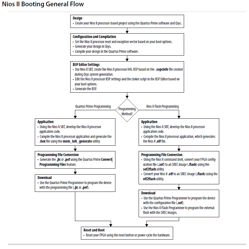
You need to get the compiled code using one of the methods listed in the "Generic Nios II Booting Methods User Guide" document I think the .hex file looks the most promising.

Load the memory from the JTAG, this document describes how to write to memory and other avalon MM devices.

Point your reset memory vector in the NOIS processor to the boot address in your external ram.

Then your going to have to trigger a reset without resetting the external ram. This is the hack part, since I don't know your setup, your going to have to do this.

Good luck, sounds like a fun project. I'd try it out if I had the time, maybe I will someday (I've also ran into this problem, for me it was much less time consuming and cheaper to upgrade the FPGA, in fact if your developing you should almost always use the biggest fpga possible)

Here is another cool article on booting from an external processor

\$\endgroup\$
1
\$\begingroup\$

During development, you don't need to have flash at all to run your code from external RAM. The debugger will load the code there and run the CPU from that location. You only need to deal with flash when you want your code to survive a shutdown.

If you do need flash, you should be aware some flash controllers support direct code execution while others don't. With the first class, you can forego the bootloader (called boot copier in the documentation) and run the code directly from flash, which saves you RAM but is often significantly slower. With the second class, you have no choice but to use the boot copier and run your code from RAM.

A typical example of the second class is the Legacy EPCS controller. It maps a small ROM containing the boot copier into the address space, so CPU reset vector should point to it in order to get your code into RAM on reset. Notably, this controller is designed in a way enabling you to keep both the FPGA configuration and your code in the same flash device. As a result, the procedure for flashing your code is somewhat complicated.

An example of the first class is the newer EPCQ controller. Unlike EPCS, it maps the entire flash contents into the memory space, which is required for in-place execution. You can still choose to put a boot copier in it and run your code from RAM to achieve faster execution speed. The Embedded Peripherals IP User Guide explains you how to choose between the two options:

The Nios II SBT tools know whether to append a boot copier based on the .text linker section location. If the .text linker section is located in a different memory than where the reset vector points, it indicates a code copy is required. At this scenario a boot copier is required. You can use the existing logic to generate a programming file with or without a boot copier depending on the scenario.

In case you don't know, linker sections are configured in the Board Support Package configuration dialog.

\$\endgroup\$
4
  • \$\begingroup\$ Thanks. The purpose of the question was to get a solution to the problem of having insufficient on chip RAM during development, which forces one to use an off chip solution. However, that solution must be supported be Altera to be feasible. \$\endgroup\$
    – quantum231
    Commented Jan 20, 2018 at 11:51
  • \$\begingroup\$ @quantum231 Alter provides plenty of SDRAM / DDR controllers for Qsys, so I don't see what's the problem. Do you have external RAM on your dev board? \$\endgroup\$ Commented Jan 20, 2018 at 12:05
  • \$\begingroup\$ There is SDRAM, SRAM and Flash (also used for configuration). \$\endgroup\$
    – quantum231
    Commented Jan 20, 2018 at 12:08
  • \$\begingroup\$ Are SDRAM or SRAM controllers included in your Qsys system? If yes, do they work? If not, why not? \$\endgroup\$ Commented Jan 20, 2018 at 12:26

Your Answer

By clicking “Post Your Answer”, you agree to our terms of service and acknowledge you have read our privacy policy.

Not the answer you're looking for? Browse other questions tagged or ask your own question.