2
\$\begingroup\$

I have a cheap Altera Cyclone II EP2C5T144C8 Dev Board and a few (4) of the IO/LVDS pins are shorted to VCC or GND as shown in the schematic segment below. The pins are also brought out to headers on the board.

The only things I can think of for why they are there are:

  1. They are meant to be left non-populated (but were accidentally populated) for the user to add pull-up/pull-down resistors
  2. They are somehow helping power the FPGA

Is there any reason a direct short to VCC/GND would be desirable for an IO pin on a Dev Board? Can I remove these resistors without negatively impacting the board's performance?

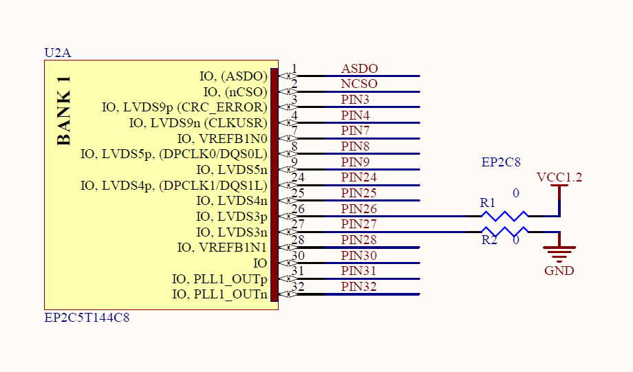
Schematic

\$\endgroup\$
6
  • \$\begingroup\$ Can you link the schematic (and ideally, the user manual)? There are multiple dev boards with that FPGA, IIRC. \$\endgroup\$
    – uint128_t
    Commented Mar 15, 2017 at 0:24
  • \$\begingroup\$ Nevermind, I'm guessing it's this one? \$\endgroup\$
    – uint128_t
    Commented Mar 15, 2017 at 0:25
  • \$\begingroup\$ @uint128_t, yes, that's the board/schematic I'm working with. There doesn't appear to be a user manual and I'm not sure where the design originated (boards available on ebay/amazon/aliexpress/etc.) \$\endgroup\$
    – ks0ze
    Commented Mar 15, 2017 at 0:40
  • \$\begingroup\$ Generally zero ohm links are used to avoid warnings/ errors generated by CAD tools for I/O signals directly connected to Power . \$\endgroup\$
    – mic
    Commented Mar 15, 2017 at 2:23
  • \$\begingroup\$ sometimes could be used as straps. there could be software that if it sees a specific pin high then it chooses some path, low it chooses some other path, or one state of a pin could mean enable something or run at a higher clock rate, use a different uart to output stuff. Logic designs could just as easily use a pin or set of pins for if-then-else so one design can have different options without re-building or re-compiling, just change the strap. \$\endgroup\$
    – old_timer
    Commented Mar 15, 2017 at 3:58

2 Answers 2

5
\$\begingroup\$

There are different packages for the FPGA. Different packages with different options.

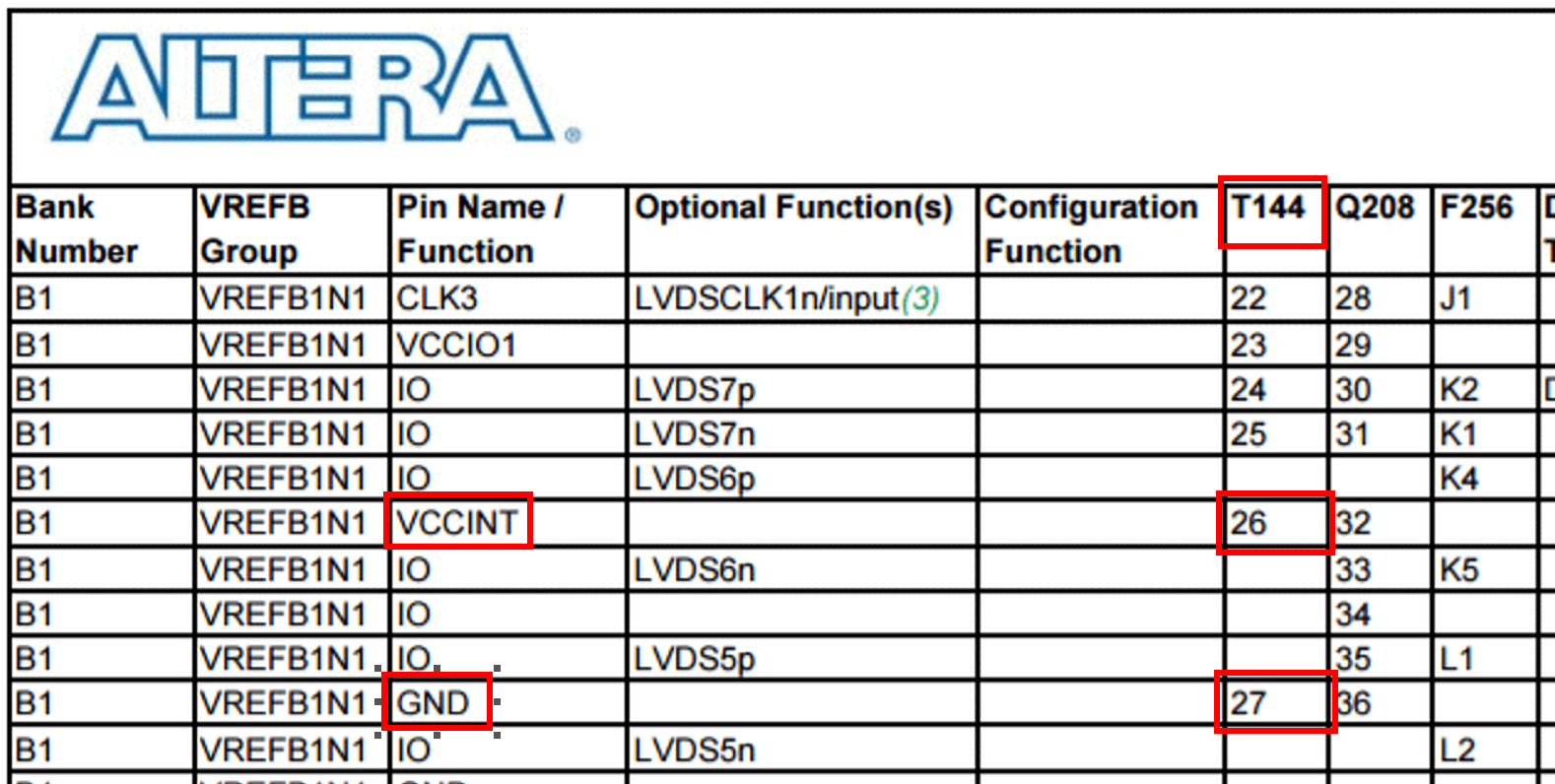
On the 144 pin EP2C8 version of the Altera Cyclone II EP2C5T144C8 Dev Board, pins 26 and 81 are VCCINT and pins 27 and 80 are GND.

The \$ 0\Omega\$ resistors allow different parts to share the same development board.

Pin Out

EP2C8 & EP2C8A Device Pin-Out

EP2C5T144 Board Diagram

\$\endgroup\$
1
\$\begingroup\$

The pinout sheet from Intel shows these to be generic I/O, no config or reference function (at least for these two, you will need to look up the other two also.) So ...

1.) They are simply for debug flexibility.

2.) They are there because the designer intended something that never came to pass.

So do a search for the net names PIN26 and PIN27 to see if they are connected to anything else that might actually need the low resistance.

If not, then don't forget to set the inputs to weak pullup to prevent floating input problems if you do decide to remove them.

\$\endgroup\$

Your Answer

By clicking “Post Your Answer”, you agree to our terms of service and acknowledge you have read our privacy policy.

Not the answer you're looking for? Browse other questions tagged or ask your own question.